Introduction
In high-frequency PCB designs, maintaining precise signal integrity requires careful attention to impedance characteristics, especially in PTFE-based boards. PTFE PCB controlled impedance ensures minimal signal reflections and losses across PTFE PCB transmission lines, critical for applications like RF and microwave circuits. Manufacturing these boards involves unique challenges due to PTFE's material properties, such as low dielectric constant and high thermal expansion. This step-by-step guide draws from factory-driven practices to help electrical engineers achieve reliable PTFE PCB impedance matching. By following structured processes aligned with industry standards, manufacturers can deliver boards that meet stringent performance demands. Understanding these steps empowers designers to collaborate effectively with fabrication teams for optimal results.
Why Impedance Control Matters in PTFE PCBs
Impedance mismatches in transmission lines lead to signal reflections, distortion, and reduced performance in high-speed circuits. PTFE PCBs excel in frequencies above 1 GHz because their low dielectric loss tangent minimizes energy dissipation, making controlled impedance essential for PTFE PCB transmission lines. Without proper control, variations in trace geometry or dielectric thickness can shift characteristic impedance, causing crosstalk or attenuation. Factory experience shows that even small deviations, like 5% changes in dielectric height, significantly impact 50-ohm lines common in RF designs. Achieving PTFE PCB impedance matching not only enhances signal quality but also ensures compliance with performance specifications in demanding environments. Electrical engineers must prioritize this during design handover to avoid costly respins.
Fundamentals of Transmission Line Impedance in PTFE Materials
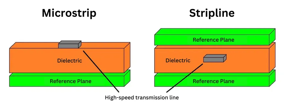
Characteristic impedance in PTFE PCB transmission lines arises from the interaction of inductance and capacitance along the conductor path. For microstrip configurations, exposed traces over a ground plane interact partially with air (Dk=1) and PTFE dielectric, yielding lower effective Dk compared to fully embedded striplines. PTFE's stable dielectric constant across frequencies simplifies predictions but requires precise control due to its softness and expansion during processing. Equations from IPC-2141 guide calculations for microstrip and stripline impedances, factoring in trace width, thickness, dielectric height, and material properties. In practice, factories model these using field solvers to account for real-world fringing fields. Understanding these principles allows engineers to specify tolerances that manufacturing can realistically achieve.
Step-by-Step Guide to PTFE PCB Controlled Impedance
Step 1: Select Appropriate PTFE Laminates
Begin with laminate selection focused on consistent dielectric properties suited for high-frequency operation. PTFE materials offer low dissipation factors, enabling efficient PTFE PCB transmission lines with reduced insertion loss. Factories verify laminate specs through standardized test methods to ensure uniformity across panels. Specify reinforced PTFE composites for better mechanical stability during lamination. Collaborate with suppliers early to confirm availability of core thicknesses that support target dielectric spacing. This foundation prevents downstream variations in PTFE PCB impedance matching.
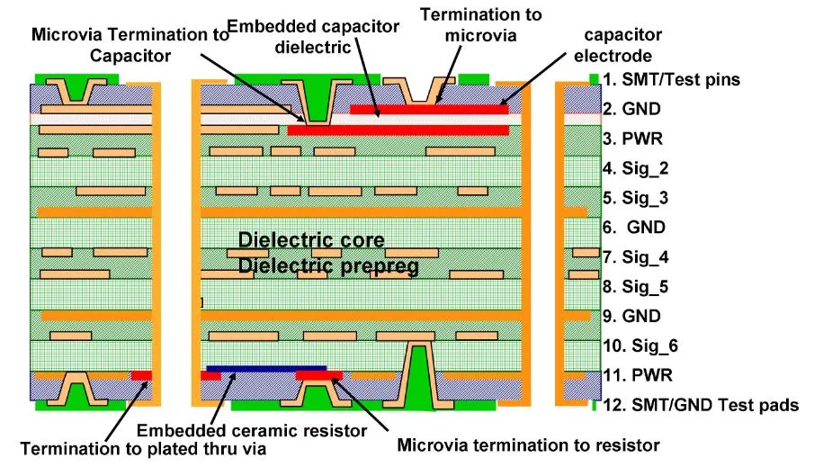
Step 2: Design the Multilayer Stackup
Develop a stackup that balances dielectric thickness, copper weights, and plane configurations for symmetric fields. Thin dielectrics increase capacitance, lowering impedance, while thicker ones raise it, ideal for adjusting to 50-ohm or 100-ohm differential pairs. Account for PTFE's higher CTE by incorporating prepreg fillers that match expansion coefficients. Simulate the stackup to predict impedance across layers, iterating for uniformity. Factories prefer even-layer counts to minimize warpage during pressing. Proper stackup design directly influences the feasibility of PTFE PCB controlled impedance.
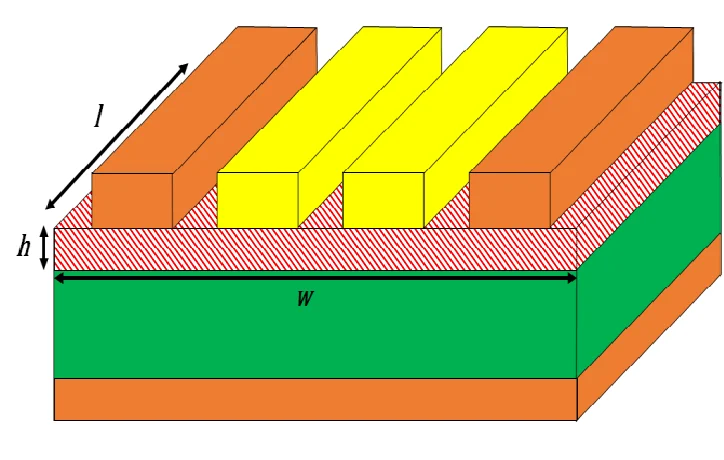
Step 3: Calculate and Specify Trace Geometry
Use design equations to determine trace widths and spacings for target impedance values. Wider traces reduce impedance by increasing capacitance, while narrower ones increase it through higher inductance. IPC-2141 provides empirical formulas tailored for PCB geometries, helping engineers set nominal values with ±10% tolerances. Include edge-to-edge spacing rules to avoid coupling between adjacent PTFE PCB transmission lines. Factories etch traces with laser direct imaging for precision, compensating for under-etch factors. Document these specs clearly in fabrication drawings to guide production.
Step 4: Implement Manufacturing Process Controls
During inner layer processing, control oxide treatments and lamination pressures to preserve dielectric integrity in PTFE boards. PTFE requires lower lamination temperatures and vacuum assistance to prevent voids that alter local capacitance. Etch control maintains trace widths within microns, critical for high-impedance lines. Outer layer imaging and plating follow similar tight tolerances, with sequential build-up for complex stacks. Post-etch cleaning removes residues that could affect surface impedance. These controls ensure the fabricated board matches design intent for PTFE PCB impedance matching.
Step 5: Verify Impedance with Testing
Post-manufacturing, perform time-domain reflectometry (TDR) to measure actual impedance along traces. TDR waveforms reveal discontinuities from vias, bends, or plating variations in PTFE PCB transmission lines. Sample multiple nets per panel to confirm uniformity, targeting specs like ±10% deviation. If discrepancies appear, correlate with cross-sections to identify thickness issues. Factories document results per IPC-6012 qualification specs for traceability. This verification step confirms PTFE PCB controlled impedance before shipment.
Best Practices and Common Challenges in PTFE Manufacturing
Adopt symmetric stackups and via stitching to stabilize ground planes, reducing impedance variations. Control solder mask application carefully, as its higher Dk can lower microstrip impedance by up to 5%. Monitor humidity during storage, as PTFE absorbs minimal moisture but panels warp under stress. Challenges like glass transition during thermal cycling demand glass-reinforced PTFE for stability. Factories use fixtures for flatness during drilling to preserve dielectric spacing. Integrating these practices yields robust PTFE PCB impedance matching.
Conclusion
Mastering impedance control in PTFE PCB manufacturing hinges on precise material handling, design rigor, and verification processes. From laminate selection to TDR testing, each step builds toward reliable PTFE PCB transmission lines with consistent performance. Electrical engineers benefit from factory insights into tolerances and challenges unique to PTFE. By aligning designs with standards like IPC-2141 and IPC-6012, teams minimize risks and accelerate high-frequency product development. Implementing this guide ensures signal integrity in demanding applications. Prioritize collaboration between design and fabrication for superior outcomes.
FAQs
Q1: What is PTFE PCB impedance matching and why is it critical?
A1: PTFE PCB impedance matching involves designing traces and stackups to achieve target characteristic impedance, preventing reflections in high-frequency signals. In PTFE PCB transmission lines, mismatches cause attenuation and crosstalk, degrading RF performance. Factories achieve this through tight etch and thickness controls, verified by TDR. Proper matching supports data rates beyond 10 Gbps reliably.
Q2: How do PTFE materials affect controlled impedance in PCBs?
A2: PTFE's low and stable dielectric constant simplifies PTFE PCB controlled impedance compared to FR-4, with less variation over temperature. Transmission lines benefit from minimal loss tangent, ideal for microwave apps. Manufacturing requires special lamination to maintain dielectric height uniformity. Engineers specify based on IPC-2141 equations for accurate predictions. Challenges include warpage mitigation during processing.
Q3: What manufacturing steps ensure accurate PTFE PCB transmission lines?
A3: Key steps include stackup design for dielectric spacing, precise etching for trace geometry, and vacuum lamination to avoid voids in PTFE layers. Factories control copper plating thickness to stabilize inductance. Post-process TDR testing confirms impedance within specs. Symmetric builds reduce asymmetry effects. This approach delivers consistent PTFE PCB impedance matching for high-speed designs.
Q4: How can engineers troubleshoot impedance deviations in PTFE PCBs?
A4: Examine TDR traces for step changes indicating thickness or etch issues in PTFE PCB transmission lines. Cross-section analysis reveals dielectric variations. Adjust stackup or trace widths iteratively using simulation tools. Factories recommend test coupons for early detection. Adhering to IPC-6012 verification prevents field failures in controlled impedance boards.
References
IPC-2141A — Design Guide for High-Speed Controlled Impedance Circuits on Printed Boards. IPC.
IPC-6012E — Qualification and Performance Specification for Rigid Printed Boards. IPC, 2017.
IPC-2221B — Generic Standard on Printed Board Design. IPC.