Introduction
In modern electronics production, automated manufacturing lines dominate PCB assembly processes, demanding designs that seamlessly integrate with high-speed pick-and-place machines, reflow ovens, and inspection systems. Optimizing PCB design for automated manufacturing begins with Design for Manufacturability (DFM) principles tailored to automation, ensuring minimal errors and maximum throughput. Engineers must consider how every layout decision impacts robotic handling, solder paste application, and optical alignment from the outset. Poorly optimized designs lead to frequent stops, rework, and yield losses, while well-prepared ones enable just-in-time production cycles. This article explores PCB design rules for automated assembly, best PCB layout practices for automation, Gerber file optimization for automation, and CAD/CAM strategies for PCB automation. By adhering to these guidelines, electric engineers can produce boards that flow effortlessly through automated facilities.
What Is DFM for PCB Automation and Why It Matters
DFM for PCB automation refers to the systematic application of design guidelines that align with the capabilities and tolerances of automated fabrication and assembly equipment. It encompasses rules for component placement, trace routing, panelization, and data output to prevent issues like misalignment or insufficient clearances during machine operations. In automated environments, where human intervention is minimal, even minor deviations can halt production lines, amplifying costs exponentially. Implementing DFM early reduces scrap rates, shortens lead times, and supports scalability for high-volume runs. Industry standards like IPC-2221 provide foundational criteria for conductor spacing and hole sizes, ensuring compatibility with automated drilling and etching processes. Ultimately, DFM bridges the gap between design intent and manufacturing reality, fostering reliable outcomes in fast-paced automation settings.
The relevance intensifies as automation advances, with surface-mount technology (SMT) lines processing thousands of components per hour. Designs ignoring automation constraints risk tombstoning, bridging, or floating components due to imprecise stencil apertures or placement offsets. Conversely, DFM-optimized boards achieve higher first-pass yields, critical for competitive electronics sectors. Engineers benefit from structured checklists that verify automation readiness before tape-out.
Key PCB Design Rules for Automated Assembly
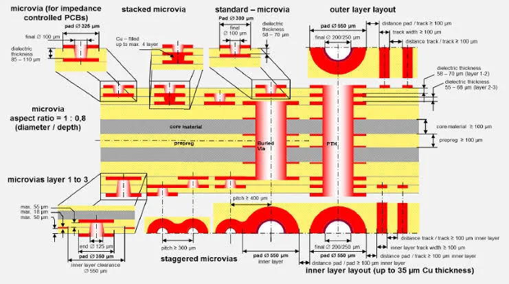
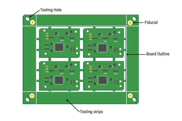
PCB design rules for automated assembly prioritize machine accessibility, precision, and repeatability across all stages from fiducial recognition to final soldering. Minimum clearances between components must accommodate nozzle sizes typically used in pick-and-place systems, preventing collisions during high-speed operations. Fiducial marks, essential for optical alignment, should be placed at three corners of the board or panel, with diameters around 1 mm and clear zones free of nearby features. Polarization notches or tabs aid robotic handling, while consistent component orientation streamlines feeder setup. Adhering to these rules minimizes programming time for assembly machines and enhances accuracy.
Trace widths and annular rings follow standardized minimums to withstand automated plating and etching variations. Vias and holes require precise aspect ratios to ensure reliable drilling by automated CNC machines, avoiding barrel cracks. Solder joints benefit from land pattern geometries that promote uniform paste volume, reducing defects in reflow. These rules collectively form a robust framework for seamless automated assembly.
Best PCB Layout Practices for Automation
Best PCB layout practices for automation emphasize symmetry, standardization, and flow optimization to support uninterrupted machine processing. Group similar components by type and height to allow efficient feeder loading and reduce changeovers between placements. Maintain unidirectional flow from left-to-right or top-to-bottom, aligning with typical conveyor directions in assembly lines. Avoid irregular board outlines that complicate automated depaneling; opt for rectangular shapes with rounded corners for smooth edge routing. Balanced copper distribution across layers prevents warpage during reflow, a common issue in automated thermal profiling.
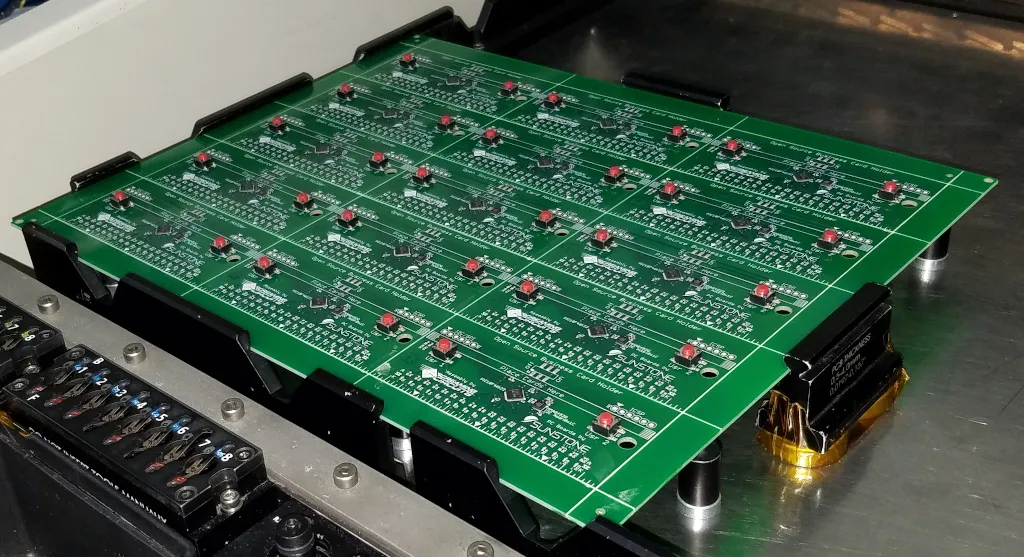
Panelization multiplies throughput by arraying multiple boards, incorporating breakaway tabs and v-scoring for easy separation post-assembly. Place test points at board edges with adequate spacing for probe access, facilitating automated in-circuit testing. Thermal pads under large components require via stitching to dissipate heat evenly, ensuring reflow ovens process boards uniformly. These practices not only boost automation efficiency but also align with quality benchmarks like IPC-A-600 for visual acceptability.
Layer stackups demand symmetry to mitigate bowing, with core and prepreg thicknesses matched on outer layers. Signal integrity considerations, such as controlled impedance traces, integrate naturally without compromising automation. Engineers should simulate layout impacts using design rule checks early.
Gerber File Optimization for Automation
Gerber file optimization for automation ensures data integrity for CAM software, enabling precise toolpath generation without manual corrections. Use RS-274X format exclusively, embedding apertures directly to eliminate separate files and reduce errors. Define units consistently as metric or imperial with sufficient decimal places, such as 3:3 for microns, to match automation tolerances. Include dedicated layers for each element: top/bottom copper, soldermask, silkscreen, paste, and drill charts in Excellon format. Name files systematically, like TOP_COPPER.gbr, to automate layer mapping in fabrication software.
Omit unnecessary apertures and flash pads, optimizing for minimal D-code count to speed CAM processing. Verify polarity and mirror settings to prevent inverted images that disrupt etching. Generate outline layers explicitly for routing and scoring paths, specifying tool sizes accurately. Post-generation, validate files with viewers to confirm layer registration and no missing data. Optimized Gerbers translate to faster setup times and fewer iterations in automated lines.
CAD/CAM Integration for PCB Automation
CAD/CAM for PCB automation requires seamless data exchange, where design software outputs directly feed manufacturing plotters and routers. Implement design rule checks (DRC) enforcing automation minima, such as pad-to-pad spacing and hole-to-trace clearances. Export stackup details in a dedicated fab drawing, detailing materials and thicknesses for precise lamination cycles. CAM engineers rely on clean ODB++ or IPC-2581 formats for intelligent data, though Gerber remains prevalent; ensure compatibility by testing exports.
Automation thrives when CAD models include 3D step files for assembly verification, allowing simulation of pick-and-place paths. Address potential issues like overlapping apertures or unplated holes through iterative reviews. J-STD-001 guidelines influence CAM programming for soldering profiles, ensuring joint reliability. This integration minimizes handoffs, accelerating from design to production.
Common Challenges and Troubleshooting in Automated PCB Production
Designs occasionally encounter hurdles like insufficient fiducial contrast, resolved by surrounding marks with soldermask-free zones. Component shadowing during AOI inspection arises from dense layouts; space tall parts adequately. Warpage from asymmetric stacks warps boards off-flatness, detectable via shadow moiré per IPC standards. Troubleshooting involves DFM audits pre-production, adjusting layouts iteratively.
Stencil misalignment from paste layer offsets demands exact registration marks. Automated depaneling fails on thin tabs; reinforce with mouse bites. These fixes, rooted in proactive design, sustain line speeds.
Conclusion
Optimizing PCB design for automated manufacturing hinges on DFM for PCB automation, rigorous PCB design rules for automated assembly, and meticulous best PCB layout practices for automation. Gerber file optimization for automation and thoughtful CAD/CAM for PCB automation complete the ecosystem, yielding high-reliability boards. Electric engineers adopting these strategies reduce defects, enhance yields, and support scalable production. Prioritize standards compliance and validation to future-proof designs against evolving automation.
FAQs
Q1: What are the core elements of DFM for PCB automation?
A1: DFM for PCB automation focuses on fiducials, component spacing, panelization, and symmetric stackups to align with pick-and-place and reflow machines. It prevents misalignment and warpage, ensuring high throughput. Follow IPC guidelines for clearances and annular rings. This approach cuts rework by streamlining machine interactions.
Q2: How do PCB design rules for automated assembly improve yields?
A2: PCB design rules for automated assembly specify minimum distances for nozzles, consistent orientations, and test point placements. They enable precise robotic handling and optical inspection. Balanced layouts avoid thermal issues in reflow. Resulting boards process flawlessly, boosting first-pass success.
Q3: Why is Gerber file optimization for automation essential?
A3: Gerber file optimization for automation uses RS-274X with embedded apertures and precise coordinates for error-free CAM import. It includes all layers and drill files systematically. Validation prevents mismatches. Optimized files accelerate fabrication setup and reduce iterations.
Q4: What role does CAD/CAM play in PCB automation?
A4: CAD/CAM for PCB automation facilitates DRC enforcement and direct data transfer to manufacturing tools. It supports 3D simulations for assembly feasibility. Clean exports minimize manual edits. Integration per J-STD-001 ensures soldering compliance and production efficiency.
References
IPC-2221B — Generic Standard on Printed Board Design. IPC, 2012
IPC-A-600K — Acceptability of Printed Boards. IPC, 2020
J-STD-001H — Requirements for Soldered Electrical and Electronic Assemblies. IPC, 2020