Understanding Mouse Bites: A Key to Efficient PCB Manufacturing
Delve into mouse bites in PCB design—their purpose, benefits for panelization, and how they compare to V-scoring for board separation and cost efficiency.
Printed Circuit Boards (PCBs) form the backbone of modern electronics, serving as the essential platform where components connect to create functional devices. In the PCB Manufacturing category, readers gain access to a comprehensive collection of resources designed to demystify the intricate processes involved in producing these critical elements. From initial design considerations to final assembly and testing, this category covers every stage, providing valuable insights for engineers, hobbyists, and industry professionals alike. Understanding PCB manufacturing is crucial for anyone involved in electronics development. This field encompasses a wide range of topics, including material selection, such as FR-4 substrates and advanced laminates, as well as fabrication techniques like etching, drilling, and soldering. Articles here delve into best practices for optimizing layouts to minimize signal interference, ensuring reliability in high-stakes applications. Tutorials guide users through prototyping methods, while in-depth analyses explore emerging trends like flexible PCBs and additive manufacturing, which are revolutionizing industries from consumer gadgets to aerospace systems. The practical value of mastering PCB manufacturing extends to real-world scenarios, where efficient production can reduce costs, enhance performance, and accelerate time-to-market. For instance, insights on multilayer board construction help in designing compact devices for IoT applications, and discussions on quality control standards prevent common pitfalls in mass production. By engaging with the diverse guides and expert perspectives in this category, readers can build a solid foundation in PCB technologies, apply proven strategies to their projects, and stay ahead in an ever-evolving field. Whether troubleshooting assembly issues or exploring sustainable manufacturing practices, the knowledge shared here empowers informed decision-making and innovation in electronics.
Delve into mouse bites in PCB design—their purpose, benefits for panelization, and how they compare to V-scoring for board separation and cost efficiency.
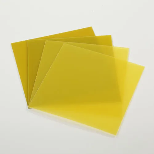
Learn best practices for prepreg storage in PCB manufacturing, including temperature, humidity, and shelf life, to prevent defects like delamination and ensure high-quality circuit boards.
Understand the differences between 1oz and 2oz copper in PCB design, including current capacity, thermal management, and cost implications, to make informed engineering decisions.
Understand solder joint voids in PCBs, including their causes, detection methods like X-ray inspection, and effective prevention strategies for robust electronic assemblies.
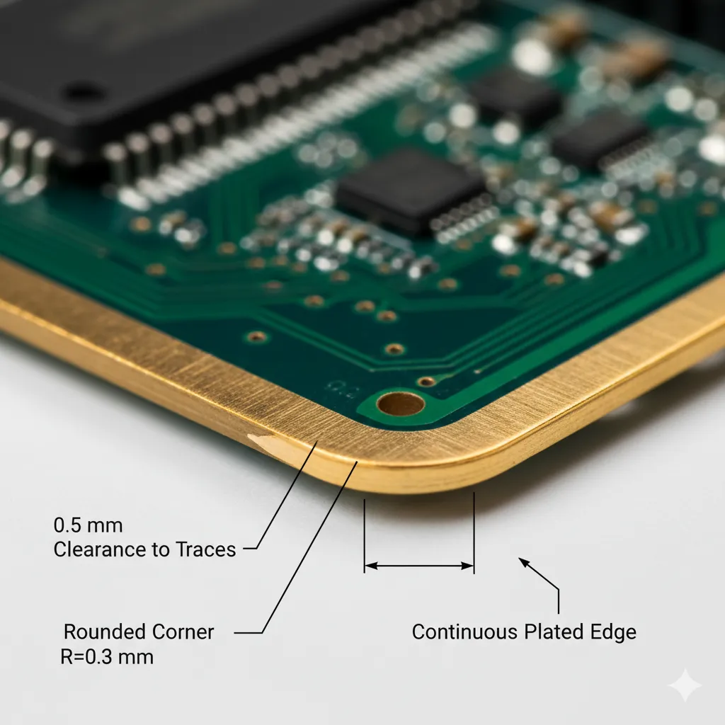
Electrical engineers can master PCB edge plating for enhanced EMC, grounding, and thermal management. Learn design rules, specifications, and best practices.
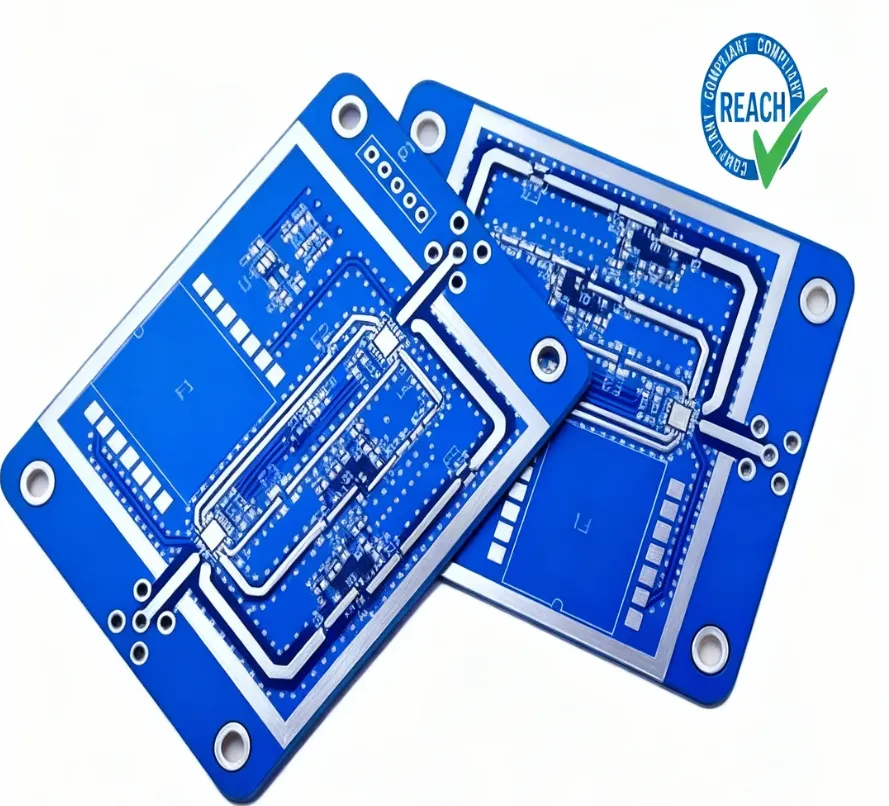
Essential insights for electronics engineers on REACH compliance in PCB design. Learn about restricted substances, the "certification" process, and material choices to ensure your PCBs meet EU regulations.
Discover effective solutions for common PCB gold finger issues like peeling, corrosion, and adhesion to ensure reliable, high-quality circuit board connections.
Discover strategies for breakaway tab stress analysis and PCB depanelization stress reduction to protect components and ensure board integrity during manufacturing.
Learn how to fine-tune laser drilling parameters for FR-4, Rogers, ceramic, PTFE, and metal core PCBs to achieve superior hole quality and manufacturing precision.
Explore essential AOI lighting techniques, types, and angles to optimize defect detection and enhance PCB inspection accuracy in manufacturing.