Introduction
In high-frequency applications such as RF and microwave circuits, printed circuit boards must deliver signals with minimal distortion and attenuation. Even trace amounts of contamination can introduce significant signal loss, compromising overall system performance. PCB cleaning for high-frequency circuits emerges as a critical process to remove residues from manufacturing, assembly, or handling. This ensures reliable impedance control and preserves the integrity of transmission lines operating at GHz frequencies. Engineers focused on electric performance recognize that proactive cleaning aligns with factory quality standards to meet demanding specifications.
Why PCB Cleaning Matters for High-Frequency Circuits
Contamination on PCBs arises from various sources including flux residues, solder paste particles, handling fingerprints, and environmental dust during fabrication or storage. These contaminants alter electrical properties, leading to signal loss due to PCB contamination that manifests as increased insertion loss or reflections. In RF circuits, where wavelengths approach millimeter scales, such issues directly impact phase stability and power efficiency. Proper cleaning restores surface uniformity and prevents long-term degradation like electrochemical migration. Factory processes emphasize cleanliness to comply with performance classes defined in standards like IPC-6012E, which outline qualification for rigid printed boards.
High-frequency signals travel primarily on conductor surfaces due to skin effect, making surface cleanliness paramount. Residues increase effective surface roughness, elevating resistive losses at frequencies above 1 GHz. Dielectric contamination absorbs moisture, raising the dissipation factor and causing additional attenuation. Without thorough cleaning, these effects cascade into crosstalk and reduced signal-to-noise ratios in dense RF layouts.
Mechanisms of Signal Loss from PCB Contamination
At high frequencies, conductor losses dominate through skin effect, where current confines to a thin outer layer of traces. Contaminants like ionic salts or organic films roughen this layer, increasing path length and resistance, thus amplifying attenuation. Corrosion products from flux activation further exacerbate this by forming non-uniform oxide layers. In practice, even nanometer-scale residues shift characteristic impedance, causing mismatches in controlled 50-ohm lines common in RF designs.
Dielectric losses intensify when polar contaminants infiltrate laminate interfaces, elevating the effective loss tangent. Moisture trapped by hygroscopic residues heightens this effect, leading to frequency-dependent signal degradation. Leakage currents from ionic contamination bridge closely spaced traces, promoting dendrite formation under voltage bias. These mechanisms collectively degrade return loss and insertion loss, critical metrics for high-frequency performance. Engineers observe these issues in vector network analyzer measurements post-contamination exposure.
Particulate matter introduces capacitive coupling and scattering, further distorting signal propagation. In multilayer high-frequency stacks, vertical migration of contaminants between layers compromises via integrity. Addressing these requires targeted cleaning strategies that eliminate all contaminant types without introducing new defects.
Best PCB Cleaning Methods for RF Circuits
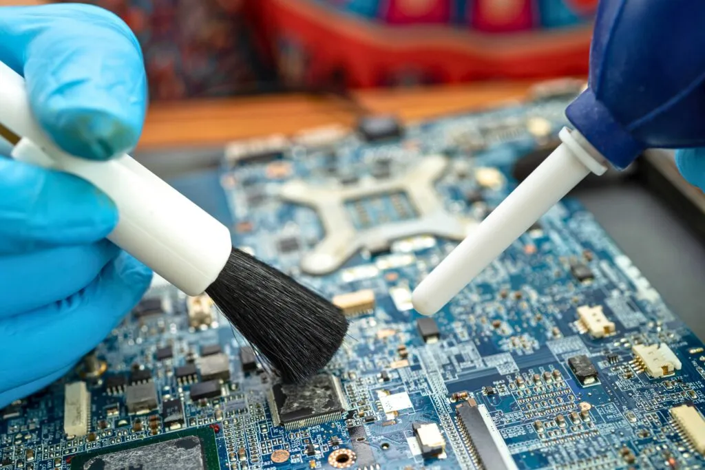
Selecting the best PCB cleaning methods for RF circuits prioritizes residue-free results while protecting fine-pitch features and sensitive laminates. Manual cleaning with high-purity isopropyl alcohol (IPA) at 90 percent or higher concentration offers a gentle starting point, applied via soft brushes or lint-free swabs to dislodge flux and particulates. This method evaporates cleanly, minimizing recontamination risks. For thoroughness, spray application under magnification ensures access to under-component areas without mechanical stress.
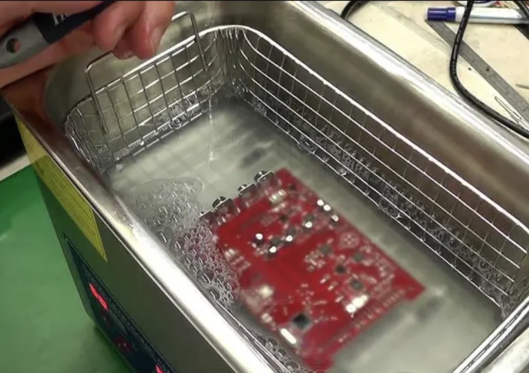
Ultrasonic cleaning accelerates contaminant removal using cavitation bubbles generated by sound waves above 40 kHz, as recommended in industry cleaning guidelines. Low-power settings prevent damage to thin copper traces or delamination in high-frequency materials. Immersion in a compatible aqueous or semi-aqueous solution, followed by deionized rinse, suits heavier residues while maintaining compatibility with RF substrates. Drying via forced hot air or vacuum completes the cycle to avoid moisture traps.
Vapor degreasing provides uniform cleaning for complex geometries, condensing solvent vapors to dissolve and carry away soils. This technique excels in controlled factory environments for batch processing RF prototypes. Each method demands validation to confirm no alteration to surface finishes critical for skin effect performance.
Impedance Control in PCB Cleaning Processes
Impedance control in PCB cleaning safeguards the precise trace geometries designed for 50-ohm or 100-ohm differential lines in high-frequency circuits. Aggressive solvents risk etching copper, widening traces and lowering characteristic impedance. Factory protocols select low-residue cleaners that neither swell dielectrics nor deposit films altering propagation velocity. Post-clean verification confirms stability within 5 percent tolerance, essential for matching networks.
Cleaning must preserve plating integrity on microstrip lines, as surface changes amplify losses at multi-GHz bands. Thorough rinsing eliminates extractable ions that could migrate under field stress, maintaining consistent Z0. Drying techniques like nitrogen purge prevent watermarks that mimic contamination effects. Integrating these steps ensures cleaning enhances rather than degrades RF signal fidelity.
Testing PCB Performance After Cleaning
Testing PCB performance after cleaning quantifies improvements in signal integrity and verifies compliance with cleanliness thresholds. Resistivity of solvent extract (ROSE) testing, outlined in IPC TM-650 method 2.3.25, extracts ionic residues into an IPA-deionized water solution for conductivity measurement. Low readings indicate effective removal of activatable contaminants prone to causing leakage in humid environments. This serves as a quick go/no-go check in production lines.
Surface insulation resistance (SIR) testing per IPC TM-650 method 2.6.3.3 evaluates long-term reliability by applying bias across comb patterns under elevated humidity and temperature. Values exceeding specified minima confirm insulation stability for high-density RF boards. For frequency-specific validation, time-domain reflectometry (TDR) scans traces to detect impedance discontinuities introduced or resolved by cleaning.
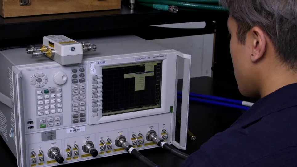
Vector network analyzer (VNA) measurements provide ultimate proof, comparing S21 insertion loss and S11 return loss before and after. Reduced attenuation post-cleaning directly correlates with minimized signal loss due to PCB contamination. These tests align factory outputs with performance specifications, enabling iterative process refinement.
Troubleshooting Common Issues in High-Frequency PCB Cleaning
Persistent residues after initial cleaning often stem from shadowed areas under components or incompatible fluxes. Increasing dwell time in ultrasonic baths or switching to vapor methods resolves this without mechanical abrasion. Impedance shifts may trace to incomplete drying, addressed by extended bake-out at moderate temperatures. Factory data logs from ROSE and SIR tests guide adjustments, ensuring repeatability.
Over-cleaning risks include laminate microcracking from excessive cavitation, mitigated by frequency tuning above 40 kHz. Cross-contamination from shared baths requires dedicated tooling per alloy or flux type. Regular calibration of test equipment maintains accuracy in performance assessments.
Conclusion
Effective PCB cleaning for high-frequency applications directly minimizes signal loss and maximizes performance by eliminating contaminants that degrade conductor and dielectric properties. Implementing best practices like IPA manual cleaning, ultrasonic immersion, and vapor degreasing, combined with rigorous impedance control, yields reliable RF circuits. Post-clean testing via ROSE, SIR, TDR, and VNA confirms success, aligning with industry benchmarks. Engineers benefit from these factory-driven approaches to achieve superior signal integrity in demanding environments.
FAQs
Q1: What causes signal loss due to PCB contamination in high-frequency circuits?
A1: Signal loss due to PCB contamination in high-frequency circuits arises from increased skin effect losses due to surface roughness, elevated dielectric dissipation from moisture-laden residues, and leakage currents from ionic salts. These effects heighten insertion loss and reflections, particularly above 1 GHz. Proper identification via visual inspection and ROSE testing guides targeted removal to restore performance.
Q2: What are the best PCB cleaning methods for RF circuits?
A2: The best PCB cleaning methods for RF circuits include high-purity IPA for manual application, ultrasonic cleaning at over 40 kHz for thorough residue removal, and vapor degreasing for uniform coverage. These preserve trace integrity without introducing new contaminants. Selection depends on residue type and board complexity, always followed by drying and verification.
Q3: How does impedance control in PCB cleaning affect high-frequency performance?
A3: Impedance control in PCB cleaning prevents etching or residue films that alter trace width and dielectric properties, maintaining 50-ohm lines critical for RF matching. Clean processes ensure consistent propagation delay and minimal reflections. Post-clean TDR testing validates stability, directly supporting low-loss signal transmission in high-frequency designs.
Q4: What testing verifies PCB performance after cleaning in RF applications?
A4: Testing PCB performance after cleaning in RF applications involves ROSE for ionic cleanliness, SIR for insulation reliability, TDR for impedance uniformity, and VNA for S-parameters. These confirm reduced attenuation and preserved signal integrity. Sequential application from basic to advanced metrics ensures comprehensive validation aligned with quality standards.
References
IPC-5704 — Cleanliness Requirements for Unpopulated Printed Boards. IPC, 2010
IPC-TM-650 2.3.25 — Resistivity of Solvent Extract (ROSE) Test Method. IPC, 2025
IPC-6012E — Qualification and Performance Specification for Rigid Printed Boards. IPC, 2017


