Introduction
As an electronic hobbyist, you have likely sketched circuits on paper or simulated them in software, but turning those designs into real printed circuit boards (PCBs) marks a key milestone. PCB manufacturing bridges the gap between your prototype ideas and functional hardware that fits neatly into enclosures or projects. This guide walks you through the entire process, from preparing files to receiving boards ready for assembly. You will learn practical steps tailored for beginners, focusing on the PCB manufacturing process for hobbyists without needing advanced engineering knowledge. By the end, you will feel confident ordering PCBs online and understanding what happens in the factory.
Why PCB Manufacturing Matters for Hobbyists
PCBs offer reliability that breadboards and perfboards cannot match, reducing loose connections and enabling compact designs for projects like Arduino shields or sensor arrays. Manufacturing your own boards allows experimentation with custom layouts, faster prototyping, and scalability for multiple units. For hobbyists, affordable PCB manufacturing has democratized access to professional-quality boards, often in quantities as low as five pieces. This process ensures your circuits perform consistently under real-world conditions, such as vibration or heat. Understanding the manufacturing side helps you avoid costly redesigns and appreciate factory precision.
Understanding PCB Specifications
Selecting the right specifications is crucial before ordering, as they define board performance, cost, and manufacturability. Start with layer count; single-sided or double-sided boards suit most hobbyist projects, while multilayer options add complexity and expense. Board thickness typically defaults to 1.6 mm for standard FR-4 material, providing mechanical strength without excess weight. Copper weight, often 1 oz per square foot, balances conductivity and etching ease for traces down to 0.15 mm wide. Solder mask color, usually green, protects copper and prevents shorts, while silkscreen adds labels for assembly.
Surface finish options like HASL or ENIG ensure solderability; ENIG resists oxidation better for fine-pitch components. Hole sizes must exceed 0.3 mm drilled diameter to avoid registration issues during plating. Always review design for manufacture (DFM) rules from the factory, such as minimum annular ring widths around pads. These specs directly impact affordable PCB manufacturing, as simpler choices keep costs low for small runs. Factories align specifications with standards like IPC-6012E for rigid board qualification to guarantee quality.
- Layers: 1-2 - Simple routing for hobby circuits
- Thickness: 1.6 mm - Standard strength for hand assembly
- Copper Weight: 1 oz - Good for power traces up to 2 A
- Min Trace Width: 0.15 mm - Balances density and yield
- Surface Finish: HASL - Cost-effective solder joint reliability
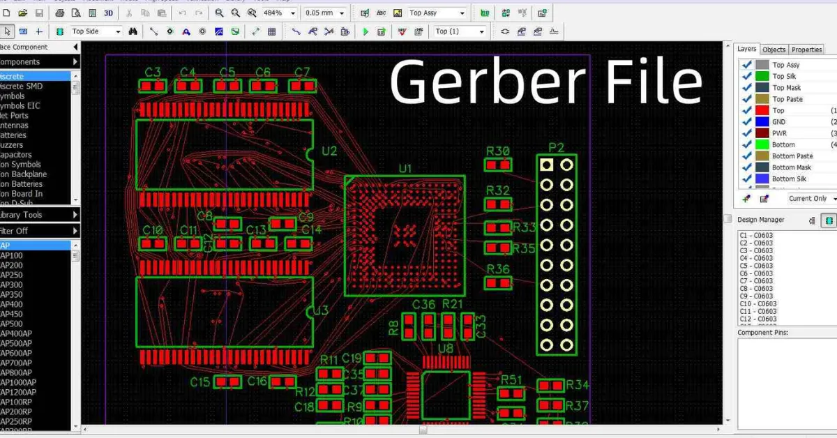
PCB Gerber Files Explained
Gerber files serve as the universal language for PCB manufacturing, converting your design software output into precise instructions for factory machines. Each Gerber file represents a layer, such as top copper for traces and pads, bottom copper for the opposite side, and solder mask layers to define exposed areas. Drill files in Excellon format specify hole locations, sizes, and plating needs, while the board outline file sets the final shape and routing paths. Netlist files verify electrical connectivity, preventing shorts or opens missed in design.
For hobbyists, generate RS-274X Gerber format, the current industry standard, avoiding older vector types. Include a drill file pair (plated and non-plated) and an aperture list for accuracy. Panelization combines multiple boards into one larger panel to reduce costs in affordable PCB manufacturing. Use free online viewers to preview files before upload, checking for overlaps or missing apertures. Factories perform automated optical inspection on these files, flagging issues early.
Choosing a PCB Manufacturer
Hobbyists benefit from manufacturers specializing in quick-turn prototypes with low minimum orders, often starting at five boards. Evaluate turnaround times, from express 24-hour options to standard 7-10 days, balancing speed with affordable PCB manufacturing. Check capabilities against your specs, such as maximum panel size or blind vias if needed later. Certifications like ISO 9001:2015 ensure consistent processes and traceability in production.
Customer reviews highlight service quality, file feedback speed, and packaging for safe shipping. Compare quotes by uploading the same Gerber set, noting inclusions like electrical testing. Prioritize those offering free DFM checks to catch design flaws pre-production. For international orders, factor in shipping times and duties, but domestic options speed up iteration cycles. Start with small batches to test reliability before scaling.
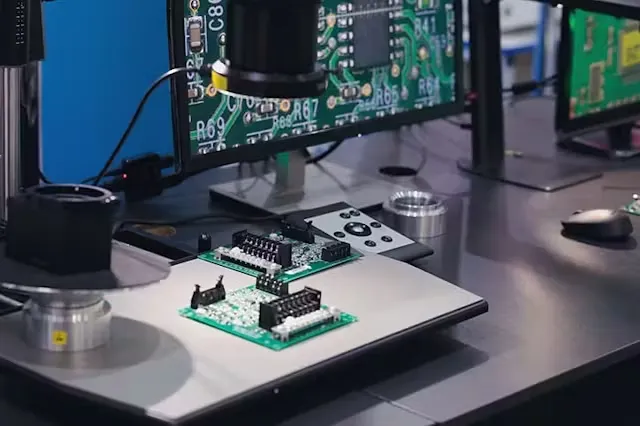
The PCB Manufacturing Process Step-by-Step
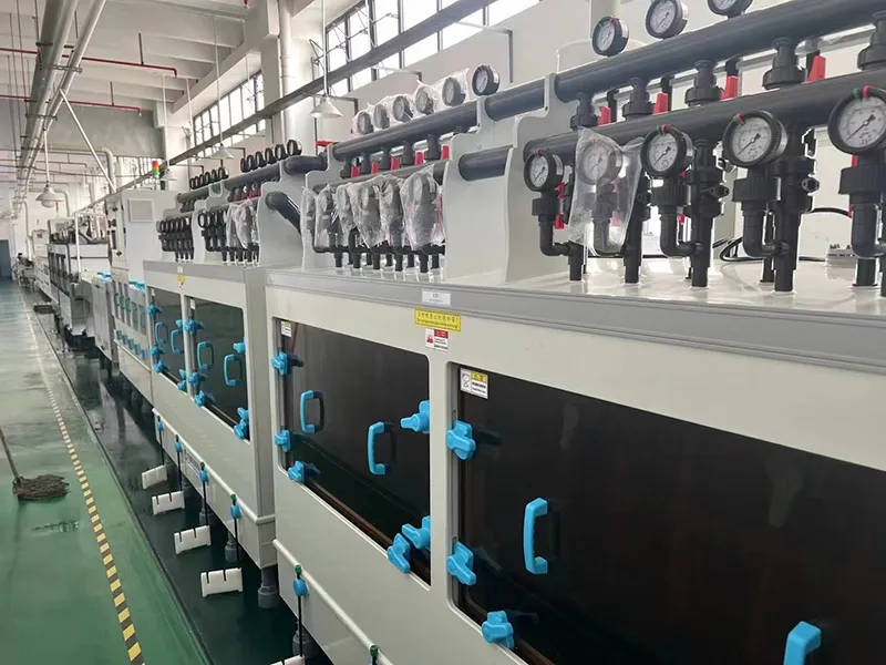
The process begins with file preparation, where engineers review Gerbers for errors and perform DFM analysis. For double-sided boards, both sides receive photoresist imaging, followed by chemical etching to remove excess copper and reveal traces. Holes get drilled using CNC machines, then electroplated with copper to connect layers via vias. Multilayer boards laminate inner cores under heat and pressure before outer processing.
Solder mask applies via screen printing or liquid photoimageable process, cured under UV light for protection. Silkscreen legends add component labels, baked for durability. Surface finish deposits a thin metal layer over exposed copper, enhancing solder wetting. Final steps include electrical testing for continuity and shorts, plus visual inspection per IPC-A-600K acceptability criteria. Boards route to shape, get scored for panels, and ship with protective packaging.
This sequence ensures high yields, with factories monitoring parameters like etch factor for uniform trace sidewalls. Hobbyists rarely need advanced options like controlled impedance, but understanding these steps explains delays or quotes.
Best Practices for Ordering PCBs Online
Upload all required files in a ZIP archive, labeled clearly, and double-check layer polarities. Select specs matching your design, opting for standard FR-4 and HASL to keep costs under 10 dollars per board for prototypes. Request panelization for multiples, saving 50 percent or more on small quantities. After quoting, review the preview panel for fit and spacing.
Communicate via the manufacturer's portal for quick clarifications on specs. Track orders online and inspect upon arrival for warpage or defects. Test a sample board electrically before full assembly. These habits streamline the PCB manufacturing process for hobbyists and build confidence in repeat orders.
Common Pitfalls and How to Avoid Them
Overlooking minimum trace spacing leads to bridging during etching, so adhere to 0.15 mm rules. Ignoring annular ring specs around vias causes plating voids; ensure at least 0.1 mm. Forgetting to merge overlapping pads in design software creates weak joints. Hobbyists often undersize power traces, risking overheating; calculate widths using online formulas conservatively.
Warped boards from improper storage result from moisture absorption, so bake if needed before assembly. Always perform incoming inspection against IPC-A-600K class 2 criteria for hobby use. These fixes prevent rework and wasted budgets.
Conclusion
Mastering PCB manufacturing empowers hobbyists to prototype reliably and iterate designs swiftly. From grasping Gerber files and specifications to navigating the online ordering process, each step builds toward professional results. Choose manufacturers wisely, follow best practices, and reference standards for quality assurance. Affordable options make this accessible, turning circuit ideas into tangible projects. Start small, learn from each run, and watch your electronics skills grow.
FAQs
Q1: What is the PCB manufacturing process for hobbyists?
A1: The process starts with Gerber file upload and DFM review, followed by imaging, etching, drilling, plating, solder mask application, and testing. Factories handle these steps for double-sided boards in days, aligning with IPC-6012E for performance. Hobbyists focus on design prep, enabling affordable prototypes under 20 dollars each. This sequence ensures reliable boards for projects like LED drivers.
Q2: How do I order PCBs online as a beginner?
A2: Select a manufacturer supporting small quantities, upload zipped Gerbers with drill files, choose specs like 1.6 mm thickness, and get an instant quote. Review the panel preview, pay securely, and track shipment. Expect 5-10 day delivery for standard runs. Free DFM feedback catches issues early, streamlining affordable PCB manufacturing.
Q3: What are PCB Gerber files and why do they matter?
A3: Gerber files detail copper layers, masks, silkscreen, and drills in RS-274X format for machine readability. They prevent misinterpretation, ensuring traces and holes match your design exactly. Include netlists for verification. Proper Gerbers are essential for choosing a PCB manufacturer and successful production.
Q4: How do I understand PCB specifications for my project?
A4: Key specs include layers, thickness, copper weight, and surface finish; match them to needs like 1 oz copper for basic circuits. Review DFM rules for min widths and hole sizes. Standards like ISO 9001:2015 guide factory compliance. Simpler choices keep costs low for hobbyists.
References
IPC-6012E — Qualification and Performance Specification for Rigid Printed Boards. IPC, 2017
IPC-A-600K — Acceptability of Printed Boards. IPC, 2020
ISO 9001:2015 — Quality Management Systems. ISO, 2015


