Introduction
Polyimide PCBs represent a cornerstone in the production of electronics designed for extreme conditions. These boards utilize polyimide materials known for their exceptional thermal stability and mechanical durability, making them ideal for demanding sectors. Engineers working on high-reliability systems often turn to polyimide substrates when standard FR4 laminates fall short. This guide explores the intricacies of polyimide PCB manufacturing, from material selection to final testing. It provides factory-level insights into processes that ensure performance under harsh environments. By understanding these elements, electric engineers can optimize designs for longevity and reliability.
What Are Polyimide PCBs and Why Do They Matter?
Polyimide PCBs incorporate polyimide as the base dielectric material, either in flexible, rigid-flex, or specialized rigid formats. Unlike conventional epoxy-based boards, polyimide offers superior resistance to elevated temperatures and repeated thermal cycling. This material choice becomes critical in applications where components face prolonged exposure to heat, vibration, and flexing. Factory production emphasizes polyimide’s role in maintaining electrical integrity over time. Its low thermal expansion coefficient minimizes stress on traces and vias during operation. For high-reliability electronics, polyimide PCBs deliver the robustness needed to meet stringent performance criteria.
The relevance of polyimide PCBs stems from their ability to outperform standard materials in challenging scenarios. In environments exceeding the limits of typical laminates, polyimide prevents delamination and warping. Manufacturers prioritize these boards for systems requiring uninterrupted service. Electric engineers value the material’s chemical resistance, which protects against solvents and fuels common in industrial settings. Overall, polyimide integration elevates PCB lifespan and reduces failure risks.
Key Material Properties Driving Polyimide PCB Performance
Polyimide materials exhibit a high glass transition temperature, allowing sustained operation in elevated thermal conditions. This property ensures dimensional stability during soldering and assembly processes. The material’s flexibility accommodates dynamic bending without cracking conductors. Factories select polyimide films or laminates based on thickness and copper cladding compatibility. Adhesiveless constructions further enhance bond strength between copper and substrate.
Mechanical strength in polyimide resists tearing and fatigue over millions of flex cycles. Electrical properties remain consistent across wide temperature ranges, supporting high-frequency signals. Chemical inertness shields the board from harsh contaminants. These attributes align with qualification requirements outlined in IPC-6013 for flexible printed boards. Engineers must consider CTE matching with adjacent materials to avoid interfacial stresses.
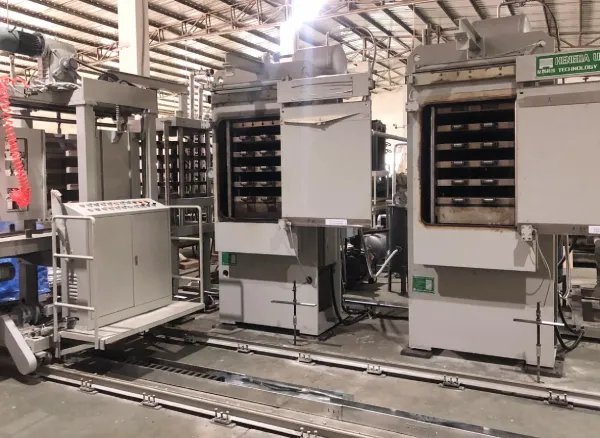
High-Temperature Polyimide PCB Manufacturing Process
The high-temperature polyimide PCB manufacturing process begins with precise material preparation. Polyimide films arrive in rolls or sheets, inspected for defects like pinholes or thickness variations. Copper foil, typically electrodeposited for flexibility, bonds to the polyimide via lamination under controlled heat and pressure. Adhesiveless laminates, preferred for high-reliability, use direct metallization to eliminate weak adhesive layers. This step sets the foundation for thermal endurance.
Photolithography follows, where dry film photoresist coats the copper surface. Exposure and development define circuit patterns aligned to design tolerances. Etching removes excess copper using chemical solutions optimized for polyimide compatibility. Factories rinse and neutralize panels to prevent residue buildup. Coverlay application protects traces, laminated similarly to the base layer.
Drilling and via formation demand laser technology due to polyimide’s toughness. Mechanical drilling risks delamination, so CO2 or UV lasers create clean holes. Electroless plating seeds vias, followed by electroplating for full copper fill. Solder mask, if required, uses polyimide-compatible inks cured at elevated temperatures. Final outline routing employs precision milling or laser cutting.
Surface finishes like ENIG or soft gold bond wires apply selectively, preserving polyimide integrity. Electrical testing verifies continuity and shorts using flying probe systems. Bake-out processes remove moisture before final inspection. Throughout, process controls monitor parameters to comply with IPC-2223 design standards for flexible boards.
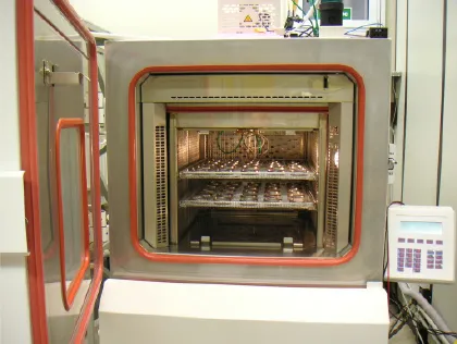
Polyimide PCB Reliability Testing Protocols
Polyimide PCB reliability testing evaluates performance under simulated operational stresses. Thermal cycling chambers expose boards to rapid temperature swings, assessing expansion mismatches. Factories measure resistance changes and visual defects post-cycles. Flex endurance tests bend samples repeatedly, checking for trace fractures via IPC-TM-650 methods. Insulation resistance holds steady, confirming dielectric reliability.
Vibration and shock simulations replicate aerospace dynamics, with accelerometers monitoring responses. Warpage assessment uses optical profilometers to quantify bow and twist limits. IPC/JEDEC-9704 guidelines aid in strain gauging critical areas like vias and bends. Humidity bias testing combines heat, moisture, and voltage to detect electrochemical migration. X-ray inspection reveals hidden voids in plating.
These protocols ensure polyimide PCBs withstand long-term degradation. Data logging tracks failure modes, informing process refinements. Electric engineers interpret results to validate designs against mission profiles.
Polyimide PCB for Aerospace Applications
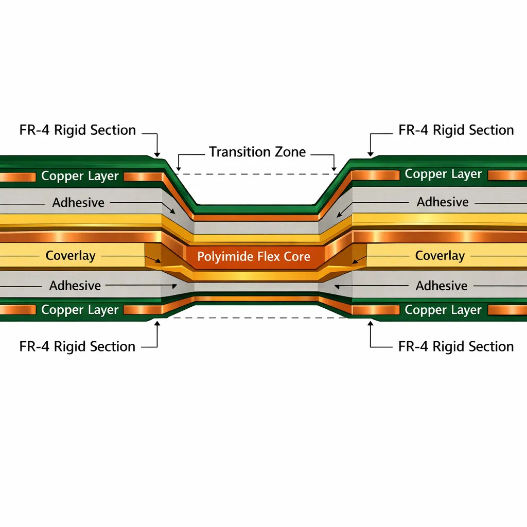
Polyimide PCB for aerospace applications powers avionics, propulsion controls, and satellite systems. Harsh conditions like engine bays demand materials resisting 200 degrees Celsius peaks and thermal shocks. Flexible polyimide variants conform to curved surfaces in aircraft structures. Rigid-flex hybrids integrate stiff sections for connectors with flexible interconnects.
Radiation hardness in polyimide suits space environments, minimizing outgassing. Vibration resistance prevents fatigue in launch phases. Factories tailor stackups for impedance control in high-speed data links. Compliance with aerospace qualifications verifies lot-to-lot consistency. These boards enable compact, lightweight designs critical for fuel efficiency.
Best Practices in Polyimide PCB Design and Production
Designers follow IPC-2223 for bend radii and trace routing to maximize flex life. Simulate thermal profiles early to predict stresses. Select polyimide grades matching application temperatures. Factories implement cleanroom handling to avoid contamination.
Layer stackup optimization balances rigidity and flexibility. Via staggering reduces stress concentrations. Process validation includes pilot runs for new designs. Solder paste selection avoids flux residue on polyimide. Final assembly uses low-temperature profiles where possible.
Common Challenges and Mitigation Strategies
Warpage arises from CTE mismatches during lamination, countered by symmetric stackups. Adhesion failures trace to surface prep; plasma treatment enhances bonding. Cost escalates with polyimide, offset by volume planning. Laser drilling burrs require optimized parameters.
Dimensional instability post-bake demands controlled cooldown. Testing throughput limits production; automated fixtures accelerate checks. Engineer collaboration with factories resolves these proactively.
Conclusion
Polyimide PCB manufacturing demands precision to unlock high-reliability potential. From material lamination to rigorous testing, each step upholds performance in extreme conditions. Electric engineers benefit from standard-aligned processes ensuring durability. Key takeaways include adhesiveless construction, comprehensive reliability protocols, and design adherence to IPC guidelines. Mastering these elements positions polyimide PCBs as go-to solutions for aerospace and beyond.
FAQs
Q1: What makes polyimide PCB for aerospace applications superior to FR4?
A1: Polyimide offers unmatched thermal stability and flex endurance, essential for avionics and satellites facing extreme temperatures and vibrations. Factory processes emphasize adhesiveless laminates to prevent delamination under thermal stress. Compliance with IPC-6013 ensures qualification for harsh environments. This reliability minimizes downtime in mission-critical systems. Engineers select polyimide for its low outgassing in vacuum conditions.
Q2: How is polyimide PCB reliability testing conducted in manufacturing?
A2: Testing involves thermal cycling, flex endurance, and strain gauging per IPC/JEDEC-9704 to simulate operational stresses. Factories monitor resistance, warpage, and insulation post-exposure. Laser inspection detects microcracks invisible to the eye. Results guide process tweaks for consistent performance. This validates boards for long-term high-reliability use.
Q3: What are the critical steps in the high-temperature polyimide PCB manufacturing process?
A3: Key steps include polyimide film lamination with copper, laser via drilling, plating, and coverlay application under vacuum. Etching and surface finishing follow strict cleanliness protocols. Bake-out removes moisture before testing. Alignment to IPC-2223 prevents defects. These ensure thermal integrity for demanding applications.
Q4: Why choose adhesiveless polyimide laminates for high-reliability PCBs?
A4: Adhesiveless designs provide stronger copper-polyimide bonds, reducing delamination risks in thermal cycling. Factories prefer them for cleaner vias and better flex life. They align with standards for aerospace-grade boards. This choice enhances overall reliability without compromising signal integrity.
References
IPC-6013DS — Qualification and Performance Specification for Flexible and Rigid-Flex Printed Boards. IPC.
IPC-2223C — Sectional Design Standard for Flexible Printed Boards. IPC.
IPC/JEDEC-9704 — Strain Gage Measurement Guideline for Printed Circuit Boards. IPC/JEDEC.