Introduction
Signal integrity in printed circuit boards (PCBs) refers to the ability of electrical signals to propagate from source to destination without distortion or degradation. In high-speed PCB design, maintaining signal integrity becomes critical as data rates increase beyond several gigabits per second. Issues like crosstalk, reflections, and jitter can lead to bit errors, system failures, and reduced performance in applications such as telecommunications, computing, and automotive electronics. Engineers must understand these challenges and employ appropriate diagnostic tools to ensure reliable operation. This article explores common signal integrity problems, diagnostic methods including eye diagrams, and strategies for mitigation through simulation and best practices. By addressing these elements, designers can optimize high-speed PCB designs for robust performance.
What Is Signal Integrity in PCBs and Why It Matters
Signal integrity encompasses the preservation of signal quality throughout the PCB interconnects, ensuring that the received waveform closely matches the transmitted one. In high-speed environments, signals behave more like transmission line waves rather than lumped circuits, making factors such as impedance control and timing alignment essential. Poor signal integrity manifests as increased bit error rates, timing violations, or electromagnetic interference, which can compromise overall system reliability. For electric engineers working on multi-gigabit interfaces, signal integrity directly impacts compliance with performance specifications and product yield. As PCB densities rise and edge rates sharpen, proactive analysis using signal integrity testing tools becomes indispensable. Ultimately, prioritizing signal integrity PCB practices enhances design margins and accelerates time-to-market.
Common Signal Integrity Issues: Crosstalk, Reflections, and Jitter
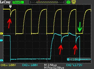
Crosstalk occurs when electromagnetic coupling between adjacent traces induces unwanted noise on a victim signal from an aggressor trace. This capacitive and inductive coupling intensifies in dense layouts with parallel routing or insufficient spacing, particularly at high frequencies. Forward crosstalk advances the victim edge, while backward crosstalk delays it, potentially causing setup or hold time violations. Engineers observe crosstalk through coupled noise peaks superimposed on the primary waveform. Mitigating it requires wider trace separations and ground shielding, aligned with design guidelines in IPC-2221. In high-speed PCB design, unaddressed crosstalk can degrade eye opening and increase jitter budgets.
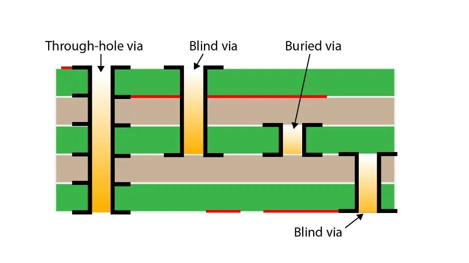
Reflections arise primarily from impedance discontinuities along the signal path, such as vias, bends, or unmatched terminations. When the incident wave encounters a mismatch, part of the energy reflects back, superimposing with subsequent waves to distort the overall shape. This ringing effect reduces signal amplitude and introduces overshoots or undershoots, exacerbating timing errors. Common sources include stubs from unused routing or abrupt width changes in traces. Proper termination resistors and smooth transitions help absorb these reflections. Reflections remain a persistent challenge in signal integrity PCB analysis, demanding precise stack-up planning. Proper differential pair routing is one of the most effective ways to reduce crosstalk—refer to our best practices for differential pair routing in high-speed designs.
Jitter represents the deviation in edge timing from an ideal position, categorized as deterministic from reflections or crosstalk, and random from noise sources. Total jitter accumulates across the channel, narrowing the timing margin for data sampling. In serial links, excessive jitter closes the eye diagram, leading to sampling errors at the receiver. Factors like power supply noise and clock instability contribute to jitter amplification in PCBs. Quantifying jitter involves separating its components for root cause analysis. For high-speed designs, jitter control ensures compliance with interface standards and reliable data recovery.
Signal Integrity Diagnostic Tools and Techniques
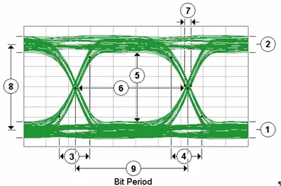
Eye diagrams provide a composite view of multiple signal transitions overlaid, revealing key metrics like eye height, width, and jitter. A wide-open eye indicates good signal integrity, while closure points to issues such as ISI or noise. Engineers generate eye diagrams using high-bandwidth oscilloscopes triggered on the data pattern, applying masks to quantify margins statistically. This visualization excels at assessing overall link quality without isolating individual impairments. In signal integrity testing tools, eye diagrams serve as a first-pass indicator before deeper dives. They guide iterative improvements in PCB layout and materials.
Time Domain Reflectometry (TDR) measures impedance profiles along traces by launching a step signal and analyzing reflections. Discontinuities appear as impedance steps or ripples in the TDR trace, pinpointing locations like vias or connectors. Correlation with physical length converts time to distance for precise fault isolation. TDR complements frequency-domain tools for pre- and post-layout verification. In high-speed PCB design, TDR validates controlled impedance targets across layers.
Vector Network Analyzers (VNAs) characterize channels via S-parameters, capturing insertion loss, return loss, and crosstalk in frequency domain. Converting to time domain yields near- and far-end crosstalk waveforms. These metrics feed into signal integrity simulation models for full-link analysis. VNAs detect subtle losses from dielectrics or surface finishes invisible in time domain. Together with oscilloscopes, they form a comprehensive suite of signal integrity testing tools.
Comparison of Signal Integrity Diagnostic Tools
| Tool | Domain | Primary Measurements | Best For | Limitations |
|---|---|---|---|---|
| Eye Diagram (Oscilloscope) | Time | Eye height/width, jitter, BER estimation | Overall link health, compliance testing | Does not isolate root causes |
| TDR | Time | Impedance profile, discontinuity location | Finding via stubs, trace mismatches | Limited to single-ended or differential pairs |
| VNA | Frequency (convertible to time) | S-parameters, insertion/return loss, crosstalk | Material characterization, full channel modeling | Higher cost, requires de-embedding expertise |
| Simulation Software | Both | Virtual eye diagrams, S-parameters, jitter | Pre-layout optimization | Depends on model accuracy |
Simulation Tools and Pre-Fabrication Analysis
Simulation is the most cost-effective way to catch PCB signal integrity issues before fabrication. Leading tools include:
- HyperLynx (Siemens) — Fast pre- and post-layout analysis with automated rule checking.
- Keysight ADS — Industry standard for channel simulation, IBIS-AMI models, and BER prediction.
- Ansys HFSS / SIwave — Full 3D electromagnetic simulation for complex via transitions and connectors.
Use IBIS or measured S-parameter models for transmitters/receivers. Perform pre-layout analysis on critical nets to optimize stack-up and routing, then run post-layout extraction including vias and connectors. Best practice is to correlate simulation results with hardware measurements on test vehicles; discrepancies greater than 10 % usually indicate model or fixture errors. Early simulation routinely reduces prototype iterations from 3–4 to 1–2.
Best Practices for High-Speed PCB Design and Signal Integrity Simulation
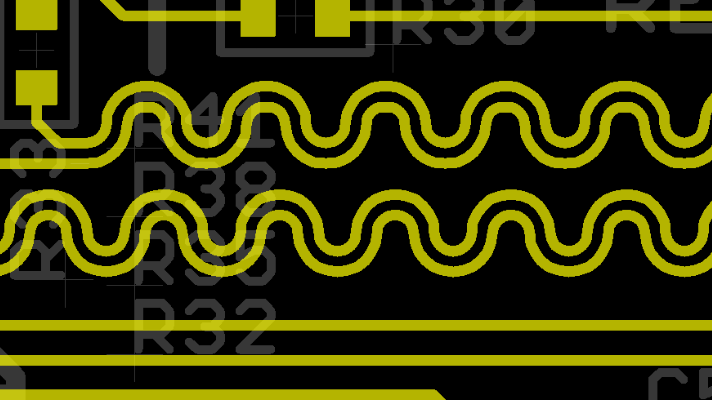
Layer stack-up design establishes reference planes and dielectric thicknesses for consistent 50-ohm or 100-ohm differential impedance. Symmetric stacks minimize warpage and intra-pair skew, crucial for balanced lines. Select low-loss dielectrics to reduce attenuation at high frequencies. Adhering to IPC-2141 guidelines ensures controlled impedance across manufacturing tolerances.
Routing strategies prioritize length matching for skew control, avoiding right-angle bends that cause reflections. Use differential pairs with tight coupling and ground vias for return path integrity. Shield sensitive nets with ground planes or guard traces to suppress crosstalk. Minimize via count and stub lengths in high-speed nets. A symmetric multilayer configuration with continuous reference planes is essential for minimizing crosstalk and maintaining impedance—see our dedicated guide on optimizing PCB stack-up for high-speed signals.
Signal integrity simulation predicts behavior pre-layout using IBIS or S-parameter models. Time-domain simulations reveal overshoot, jitter, and eye diagrams under realistic conditions. Frequency-domain analysis optimizes equalization and de-embedding. Iterate designs virtually to meet timing budgets before fabrication. This front-loading reduces respins and enhances signal integrity PCB outcomes.
Troubleshooting Signal Integrity Problems
Start with eye diagram inspection to triage dominant issues: vertical closure suggests loss or noise, horizontal indicates jitter. De-embed fixtures for accurate channel response. If reflections dominate, perform TDR to locate mismatches and adjust terminations. For crosstalk, review routing adjacency and add shielding.
Jitter decomposition via tail fitting separates random and deterministic components, tracing sources to power integrity or clocking. Simulate extracted S-parameters against measurements to validate models. Fabricate test coupons on panels for representative characterization. Systematic correlation between simulation, measurement, and layout refines designs per IPC-2221 principles.
Advanced Topics and Future Trends
At 224G PAM4, channel loss exceeds 40 dB, demanding advanced equalization, retimers, and AI-driven channel optimization. Emerging tools include machine-learning-assisted simulation that predicts optimal routing in seconds and 3D full-wave solvers that model entire boards with package and connector transitions. Quantum-inspired solvers and cloud-based SI platforms are reducing simulation times from days to hours. Engineers should prepare for tighter integration between SI, PI, and thermal analysis as systems move toward co-packaged optics and chiplets.
Conclusion
Signal integrity issues like crosstalk, reflections, and jitter pose significant hurdles in high-speed PCB design, but diagnostic tools and best practices provide effective countermeasures. Eye diagrams, TDR, and VNAs enable precise analysis, while simulation anticipates problems early. Implementing controlled impedance, optimized routing, and low-loss materials aligns with industry standards for reliable performance. Electric engineers benefit from structured workflows integrating these elements, ensuring robust signal integrity PCB implementations. Proactive attention to these factors minimizes risks and supports advanced applications.
FAQs
Q1: What causes crosstalk in signal integrity PCB designs?
A1: Crosstalk stems from electromagnetic coupling between parallel traces, with capacitive effects dominating near-fields and inductive in far-fields. Closer spacing or faster edges amplify noise transfer to victim signals. Mitigation involves increasing separation, using ground shields, and orthogonal routing layers. In high-speed PCB design, simulations predict coupling levels for layout adjustments.
Q2: How do eye diagrams help with signal integrity testing tools?
A2: Eye diagrams overlay bit patterns to visualize margin against noise and jitter, quantifying eye opening for bit error rate estimation. Masks test compliance statistically over millions of bits. They reveal combined effects of reflections, crosstalk, and loss efficiently. Engineers use them as a benchmark in signal integrity testing tools for design validation.
Q3: Why is signal integrity simulation essential for high-speed PCB design?
A3: Signal integrity simulation models full channels pre-layout, forecasting jitter, overshoot, and attenuation under load. It allows optimization of stack-up, routing, and compensation without prototypes. Comparing simulated eye diagrams to specs ensures margins. This reduces iterations and costs in high-speed PCB design.
Q4: What role do reflections play in jitter for PCBs?
A4: Reflections from impedance mismatches create deterministic jitter by modulating edge positions with ringing tails. Multiple bounces accumulate phase noise in serial links. Proper termination and via optimization per design standards minimize this contribution. Monitoring via TDR isolates reflection-induced jitter early.
References
IPC-2221 — Generic Standard on Printed Board Design. IPC
IPC-2141 — Design Guide for High-Speed Controlled Impedance Interconnects. IPC
IPC-6012E — Qualification and Performance Specification for Rigid Printed Boards. IPC, 2017