Introduction
The rapid evolution of Internet of Things (IoT) technology demands agile development cycles where engineers can iterate designs quickly. Small-batch PCB manufacturing emerges as a key enabler, allowing production of limited quantities tailored for prototyping phases. This approach minimizes upfront costs and reduces time-to-market for iot pcb design projects. For electric engineers working on wireless sensors and connected devices, it provides the flexibility to test real-world performance without committing to high-volume runs. By focusing on precision and speed, small-batch processes align perfectly with the iterative nature of modern hardware development. Ultimately, this manufacturing method transforms how teams bring IoT innovations from concept to functional prototypes.
What Is Small-Batch PCB Manufacturing and Why It Matters for IoT Prototyping
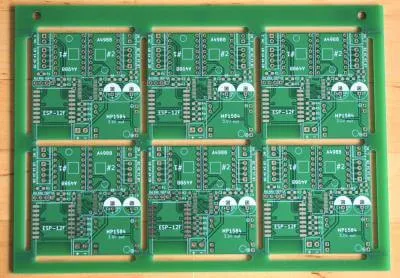
Small-batch PCB manufacturing refers to the production of printed circuit boards in low volumes, typically ranging from one to a few hundred units, with accelerated turnaround times. Unlike mass production, which prioritizes economies of scale, small-batch emphasizes customization and rapid delivery to support prototyping needs. In the context of IoT device prototyping, this method proves essential because IoT projects often involve unique layouts for pcb for wireless sensors and low power pcb manufacturing requirements. Engineers benefit from the ability to refine designs based on early feedback, avoiding the pitfalls of overproduction.
The relevance intensifies with the growing complexity of connected ecosystems, where devices must integrate seamlessly with networks. Small-batch runs facilitate thorough validation of signal integrity and power efficiency before scaling up. This directly impacts project timelines, as delays in prototyping can cascade into months of lost development time. For teams targeting battery-operated sensors, the precision in small-batch fabrication ensures compliance with design intent without excess material waste. Consequently, it revolutionizes workflows by bridging the gap between simulation and physical testing.
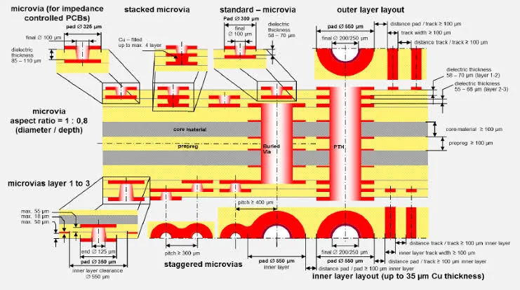
Technical Principles Behind Small-Batch PCB Production for IoT Devices
At its core, small-batch PCB manufacturing leverages optimized fabrication techniques to handle diverse specifications efficiently. Processes like direct imaging for fine-line patterns and laser drilling for vias enable high-density interconnects crucial for compact IoT modules. Material selection focuses on low-loss substrates to support low power pcb manufacturing, maintaining signal quality in wireless applications. Panelization plays a pivotal role, where multiple boards are arrayed on a single panel to maximize yield despite low volumes. This approach reduces setup costs while upholding mechanical stability during handling and assembly.
Adherence to standards such as IPC-6012E ensures qualification and performance for rigid printed boards in prototype stages. Engineers must consider thermal management principles, as IoT devices generate localized heat from RF components. Controlled impedance routing becomes critical for pcb for wireless sensors to prevent crosstalk in high-frequency bands. Fabrication tolerances tighten for small batches, often achieving trace widths below 0.1 mm through advanced etching controls. These principles collectively enable reliable prototypes that mirror production intent.
Layer stackups in small-batch runs prioritize symmetry to minimize warpage, especially for multilayer boards common in connected device pcb assembly. Vias are strategically placed to optimize current flow and reduce inductance in power planes. Solder mask application follows precise registration to protect fine-pitch components. Electrical testing, including flying probe methods, verifies continuity without fixtures, suiting low-volume needs. Such mechanisms ensure prototypes perform under real operating conditions.
Best Practices for IoT PCB Design in Small-Batch Manufacturing
Effective iot pcb design for small-batch production starts with design for manufacturability (DFM) checks early in the layout phase. Engineers should incorporate generous annular rings around pads to accommodate minor alignment variations inherent in quick-turn processes. For low power pcb manufacturing, route power and ground planes contiguously to lower resistance and enhance EMI suppression. Component footprints adhere to standard libraries, facilitating automated placement during assembly. Simulation tools verify thermal dissipation before committing to fabrication, preventing hotspots in sensor nodes.
Panelization strategies optimize material use by arranging boards with fiducials for precise registration. Include test points for in-circuit validation, streamlining debug in iot device prototyping. Copper balancing across layers mitigates stress during lamination, crucial for multilayer IoT boards. Specify controlled impedance for high-speed traces serving wireless interfaces. These practices reduce iterations, as first-pass success rates improve significantly.
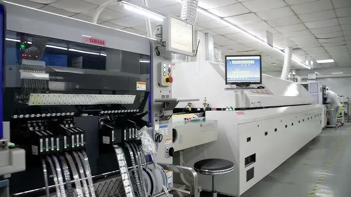
In connected device pcb assembly, prioritize surface-mount technology (SMT) compatible layouts with adequate clearances. For wireless sensors, isolate RF sections using ground pours to contain emissions. Bake-out procedures address moisture sensitivity per JEDEC J-STD-020E guidelines before reflow. Stencil design incorporates apertures tuned for low-volume paste deposition. Post-assembly inspections focus on solder joint integrity, ensuring reliability in field trials.
Challenges in Small-Batch Production and Practical Solutions
One common challenge in small-batch PCB manufacturing is achieving consistent quality across varied designs without dedicated tooling. Solutions involve rigorous incoming material inspections and process controls aligned with factory capabilities. For pcb for wireless sensors, impedance mismatches arise from substrate variations; mitigate by specifying tight dielectric constant tolerances. Yield optimization requires statistical process control to monitor plating uniformity.
Thermal cycling during soldering poses risks to delicate IoT components, potentially causing delamination. Implement ramped profiles and nitrogen atmospheres to enhance joint formation. In low power pcb manufacturing, parasitic losses from suboptimal via configurations degrade battery life; employ blind or buried vias judiciously. Documentation of Gerber files with embedded stackup details prevents misinterpretation.
Scalability from prototype to production demands foresight in material choices, favoring those qualified under IPC-A-600K for acceptability. Troubleshooting warpage involves symmetric builds and constrained baking post-fabrication. For connected device pcb assembly, handling mixed-technology boards requires hybrid fixturing. These targeted solutions empower engineers to navigate constraints effectively.
Real-World Insights: Optimizing Prototyping Workflows
Electric engineers often face pressure to accelerate iot device prototyping while maintaining robustness. A structured workflow integrates DFM reviews with small-batch orders, allowing weekly iterations. Feedback loops from assembled prototypes refine antenna tuning for wireless sensors. Low-volume runs reveal mechanical weaknesses, such as flexing in enclosures, prompting reinforcement.
Transitioning to assembly highlights paste printing yields, where 90-degree rotations aid stencil release. Power profiling post-assembly uncovers inefficiencies, guiding pcb redesigns. Collaborative reviews between design and manufacturing teams preempt issues. Such insights foster a culture of continuous improvement in IoT hardware development.
Conclusion
Small-batch PCB manufacturing fundamentally reshapes rapid prototyping for IoT devices by delivering speed, customization, and reliability. It empowers engineers to validate iot pcb design and pcb for wireless sensors through tangible iterations. Best practices in low power pcb manufacturing and connected device pcb assembly ensure prototypes transition smoothly to volume production. By embracing standards and technical principles, teams achieve higher first-pass yields and shorter development cycles. This methodology not only cuts costs but also accelerates innovation in connected ecosystems. Forward-thinking engineers will leverage these capabilities to stay ahead in competitive landscapes.
FAQs
Q1: What role does small-batch manufacturing play in iot pcb design for rapid prototyping?
A1: Small-batch manufacturing supports iot pcb design by enabling quick fabrication of custom layouts for testing wireless interfaces and power schemes. Engineers iterate designs based on performance data from physical boards, reducing simulation-prototype gaps. This approach aligns with low-volume needs, incorporating DFM to boost yields. Overall, it shortens cycles from concept to validation.
Q2: How does low power pcb manufacturing benefit wireless sensor applications?
A2: Low power pcb manufacturing optimizes trace routing and material choices to minimize losses in battery-powered wireless sensors. It ensures stable voltage delivery through solid ground planes and reduced via inductance. Prototypes reveal real efficiency metrics, guiding refinements. Standards like IPC-6012E help qualify boards for extended operation.
Q3: Why is connected device pcb assembly critical for IoT prototypes?
A3: Connected device pcb assembly validates integration of MCUs, radios, and sensors in small batches. It uncovers soldering defects and mechanical fits early, preventing scaled production issues. Techniques like precise stencil printing enhance joint reliability. This step confirms functionality under operational stresses.
Q4: What are key considerations for iot device prototyping in small batches?
A4: Key considerations include panelization for cost efficiency and test points for debug in iot device prototyping. Specify materials for RF performance and adhere to JEDEC guidelines for handling. Balance density with thermal reliefs. These ensure robust, field-ready prototypes.
References
IPC-6012E — Qualification and Performance Specification for Rigid Printed Boards. IPC, 2017
IPC-A-600K — Acceptability of Printed Boards. IPC, 2020
JEDEC J-STD-020E — Moisture/Reflow Sensitivity Classification. JEDEC, 2014