Introduction
Solder mask peeling represents a critical failure mode in printed circuit board manufacturing that compromises PCB protection and overall reliability. This delamination occurs when the solder mask layer separates from the underlying copper or substrate, exposing traces to environmental hazards like moisture, corrosion, and mechanical damage. For electric engineers working on high-density interconnects or harsh-environment applications, understanding solder mask peeling is essential to prevent field failures and costly rework. Poor solder mask adhesion not only leads to manufacturing defects but also undermines the long-term performance of assemblies under thermal cycling or vibration. Factories must prioritize root cause analysis to maintain yield rates and meet customer specifications. This article explores the mechanisms behind solder mask peeling, key contributing factors, and proven strategies for mitigation.
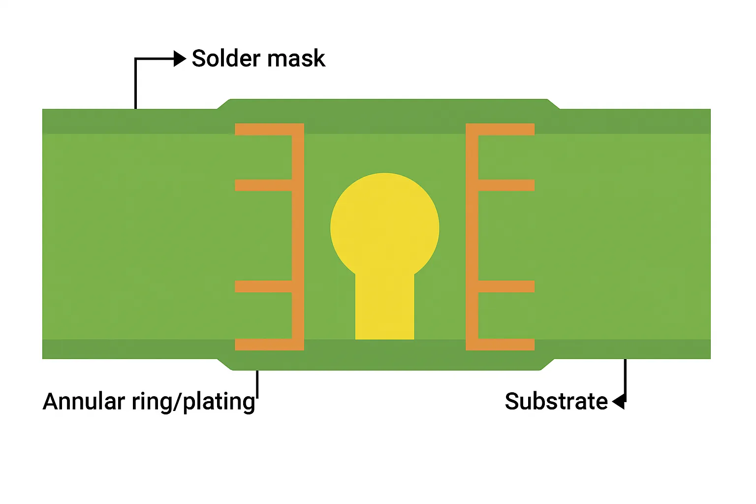
What Is Solder Mask Peeling and Why It Matters for PCB Protection
Solder mask is a thin polymer coating applied to the PCB surface to insulate copper traces, prevent solder bridging during assembly, and provide a barrier against oxidation and contaminants. Peeling refers to the partial or complete detachment of this layer, often appearing as blisters, cracks, or lifted edges visible under inspection. In terms of PCB manufacturing defects, solder mask peeling disrupts the protective integrity, allowing ionic migration or short circuits in humid conditions. Electric engineers rely on robust solder mask adhesion to ensure signal integrity and mechanical stability in multilayer boards. According to IPC standards, acceptable solder mask coverage requires uniform adhesion without delamination under specified test conditions. Neglecting this issue can escalate to assembly rejects, accelerated aging, and compliance failures in sectors like automotive or aerospace electronics.
The relevance extends beyond aesthetics; peeled solder mask exposes the board to accelerated corrosion, especially in high-reliability applications. Engineers must recognize that even minor peeling can propagate under thermal stress, leading to intermittent failures. Proper PCB protection via intact solder mask supports compliance with qualification protocols and extends operational life. Factories report that adhesion-related defects account for a significant portion of visual rejects during final inspection. Addressing solder mask peeling early in the process chain optimizes throughput and reduces scrap rates. Ultimately, strong solder mask adhesion forms the foundation of reliable PCB performance.
Root Causes of Solder Mask Peeling
Solder mask peeling stems from a combination of material, process, and environmental factors that weaken interfacial bonds between the mask and substrate. Contamination on the PCB surface prior to mask application is a primary culprit, as residues from drilling, desmear, or etching create weak boundaries that fail under stress. Oils, fingerprints, or chemical leftovers reduce wettability, preventing proper ink penetration and curing. In high-volume production, inconsistent cleaning protocols exacerbate this, leading to sporadic defects across panels. Engineers should inspect for hydrophobic surfaces using water break tests to quantify cleanliness levels. Surface contamination is one of the most common causes — see our detailed guide to solder mask misalignment causes and solutions for related adhesion issues.
Processing parameters during solder mask application and curing play a pivotal role in adhesion strength. Inadequate exposure in UV-curing systems or insufficient thermal post-bake results in incomplete polymerization, leaving the mask brittle and prone to delamination. Overexposure, conversely, can cause embrittlement or outgassing that lifts the film. Panel warpage from previous lamination steps induces tensile stresses during screen printing, promoting edge peeling. Factories must control conveyor speeds, squeegee pressure, and oven profiles to ensure uniform thickness, typically 15 to 35 microns per IPC guidelines. Variations in these steps often correlate with peeling observed in corner regions of the board.
Material incompatibilities between the solder mask formulation and base laminate further contribute to failures. Epoxy-based masks may exhibit poor bonding on polyimide substrates due to differing coefficients of thermal expansion, leading to shear during reflow. Low-durometer masks on rigid FR-4 can crack under flexure, mimicking peeling. Selection of liquid photoimageable solder mask versus dry film requires matching viscosity and cure chemistry to the panel's surface energy. Inconsistent supplier formulations across lots introduce variability, necessitating qualification testing.
Environmental factors accelerate latent weaknesses in solder mask adhesion. High humidity during storage absorbs moisture into the mask, causing blistering upon heating due to steam pressure at the interface. Temperature excursions in shipping or warehousing induce expansion mismatches, cracking the bond line. Salt-laden atmospheres in coastal facilities promote underfilm corrosion, hastening peel initiation. Engineers designing for harsh environments must consider these interactions early.
Mechanical stresses from handling, fixturing, or assembly processes can trigger peeling in marginally adhered masks. Sharp bends during depaneling or abrasive cleaning post-mask application shear the layer. Vibration testing reveals how poorly adhered masks propagate cracks under cyclic loading. Comprehensive root cause analysis combines microscopy, peel strength tests, and cross-sectioning to isolate dominant mechanisms.
Implementing Solutions for Reliable Solder Mask Adhesion
To combat solder mask peeling, factories implement rigorous surface preparation protocols starting with plasma or chemical desmear to achieve atomic-level cleanliness. Micro-etching with permanganate solutions removes oxides and smears, enhancing topography for mechanical interlocking. Post-clean rinse and dry steps, verified by contact angle measurements below 30 degrees, ensure optimal wettability. Engineers benefit from integrating these into the process flow to boost adhesion by up to 50 percent without added cost. For advanced techniques on 1 oz copper boards, follow the recommendations in our advanced solder mask techniques for 1 oz copper PCBs.
Process optimization focuses on controlled application and curing tailored to panel geometry. Automated screen printers with vision alignment minimize defects from misalignment, while zoned UV exposure compensates for warpage. Thermal profiles ramp to 150 degrees Celsius for 60 minutes post-exposure, fully cross-linking the polymer as per IPC-SM-840 qualification. Inline thickness gaugers and cure verification via differential scanning calorimetry maintain consistency. These measures directly address manufacturing defects linked to peeling.
Material selection and qualification form the backbone of reliable PCB protection. Compatibility testing per IPC-6012 involves accelerated aging, thermal shock, and adhesion pulls exceeding 5 N/cm. Opt for masks with proven track record on specific laminates, balancing flexibility and chemical resistance. Lot-to-lot traceability prevents formulation drifts that undermine solder mask adhesion.
Environmental controls mitigate external risks effectively. Climate-controlled storage at 23 degrees Celsius and 50 percent relative humidity prevents moisture ingress, with baking at 125 degrees Celsius prior to masking for moisture-sensitive boards. Packaging with desiccants and vapor barriers protects during transit. Design rules incorporating larger clearances around high-stress areas reduce peel propensity.
Testing regimes provide early detection and validation. Crosshatch adhesion tests per ASTM D3359, combined with tape pulls, screen for weak bonds post-cure. Thermal cycling from -40 to 125 degrees Celsius per JEDEC standards simulates service life, revealing latent peeling. Acoustic microscopy detects voids non-destructively. Integrating these into incoming inspection and final AOI ensures only robust boards proceed to assembly.
Troubleshooting Solder Mask Peeling in Production
When peeling emerges, systematic troubleshooting isolates the cause efficiently. Begin with visual mapping to correlate defect locations with process zones, such as edges indicating warpage or centers suggesting cure issues. Cross-sections under SEM reveal interfacial failures, distinguishing cohesive versus adhesive breaks. Contamination analysis via FTIR spectroscopy identifies organic residues.
Case patterns often point to upstream lamination defects, like voids causing local stress concentrations. Adjusting inner layer bond strength per IPC-A-600 criteria resolves these. For field returns, humidity exposure tests replicate failures, guiding design mitigations like conformal coatings over masks.
Data logging from MES systems trends peel rates against variables, enabling predictive adjustments. Collaborative reviews with material engineers refine formulations iteratively.
Conclusion
Solder mask peeling undermines PCB protection but yields to targeted interventions in surface prep, processing, materials, and testing. Electric engineers armed with these insights can specify robust designs and collaborate on manufacturing improvements. Prioritizing solder mask adhesion eliminates common defects, ensuring reliability across lifecycles. Factories adopting standard-aligned practices achieve higher yields and customer trust. Proactive measures today prevent tomorrow's failures.
FAQs
Q1: What causes solder mask peeling during PCB manufacturing?
A1: Solder mask peeling often results from surface contamination, improper curing, or material mismatches that weaken adhesion. Manufacturing defects like inadequate cleaning or warpage exacerbate the issue. Factories address this through plasma treatment and controlled thermal profiles to enhance PCB protection. Regular adhesion testing per industry standards prevents recurrence.
Q2: How can environmental factors lead to solder mask adhesion failure?
A2: High humidity and temperature swings cause moisture absorption and expansion stresses at the mask-substrate interface. These environmental factors promote blistering or delamination over time. Engineers mitigate risks with dry storage and baking protocols before application. Robust designs incorporate compatible materials for long-term stability.
Q3: What are best practices to prevent solder mask peeling in high-reliability PCBs?
A3: Implement thorough surface preparation, optimized UV/thermal curing, and compatibility qualification. Inline inspections and peel tests verify adhesion strength. These steps align with IPC guidelines, reducing manufacturing defects. Focus on process controls for consistent solder mask adhesion across production runs.
Q4: How do you test for solder mask adhesion issues early in production?
A4: Use crosshatch, tape pull, and peel strength tests post-cure to quantify bond integrity. Thermal shock and humidity exposure simulate service conditions. Acoustic imaging detects subsurface voids. Early detection allows adjustments, ensuring reliable PCB protection.
References
IPC-SM-840D — Qualification of Permanent Solder Mask. IPC, 2007
IPC-6012E — Qualification and Performance Specification for Rigid Printed Boards. IPC, 2015
IPC-A-600K — Acceptability of Printed Boards. IPC, 2020


