Introduction
Printed circuit board (PCB) manufacturing stands at the heart of the electronics industry, powering devices from consumer gadgets to industrial systems. Traditional processes often involve high energy use, chemical-intensive etching, and substantial waste generation, contributing to environmental strain. PCB automation introduces precision robotics, intelligent software, and optimized workflows that align production with sustainability goals. By focusing on eco-friendly PCB automation, manufacturers can significantly lower their ecological footprint while maintaining quality standards. This article explores how automation transforms PCB production into a greener practice, emphasizing reducing waste in PCB manufacturing and sustainable PCB assembly practices. Electric engineers benefit from understanding these shifts, as they influence design choices and supply chain decisions.
Environmental Challenges in Traditional PCB Manufacturing
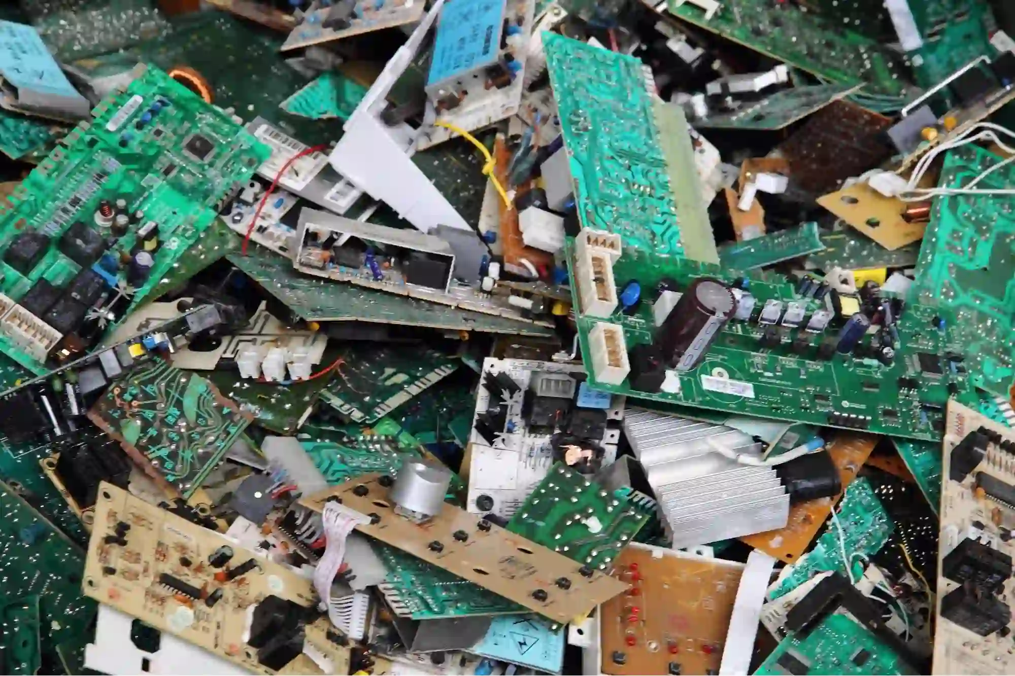
Conventional PCB fabrication relies on manual interventions and semi-automated equipment, leading to inefficiencies across multiple stages. Etching processes generate copper-laden wastewater, while drilling and lamination produce scrap materials that demand careful disposal. Energy demands peak during soldering and testing, where inconsistent operations amplify consumption. Human errors in component placement result in rework, multiplying material waste and emissions from repeated heating cycles. These factors compound the industry's carbon footprint, prompting a shift toward green PCB automation technologies. Adherence to standards like ISO 14001 helps factories systematically address these issues through environmental management.
Layer count and board complexity exacerbate resource use, as thicker stacks require more materials and longer processing times. Packaging and shipping add to the tally with non-recyclable materials. Without optimization, end-of-life disposal poses risks from hazardous substances embedded in laminates. Engineers must recognize these pain points to prioritize designs compatible with automated, low-impact flows.
How PCB Automation Mitigates Environmental Impacts
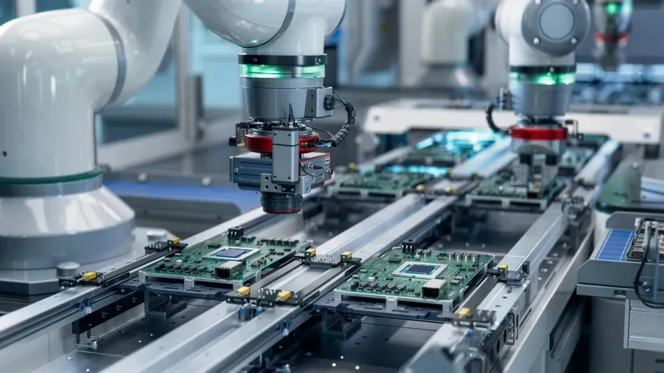
Automation replaces variability with repeatability, directly targeting waste streams in PCB production. Robotic pick-and-place machines achieve micron-level accuracy, minimizing misplacements that lead to defective boards and scrap. Vision-guided systems inspect in real-time, catching flaws early to prevent downstream waste. These technologies reduce the need for rework, conserving energy otherwise spent on reflow ovens and manual corrections. Sustainable PCB assembly practices emerge from this precision, as automated lines handle delicate components without physical strain or errors.
Energy efficiency gains come from programmed optimizations, such as dynamic speed adjustments based on board density. Idle times shorten with seamless transitions between stations, unlike manual setups prone to delays. Closed-loop feedback in automation software predicts and adjusts parameters, stabilizing processes to avoid over-etching or excess plating. Factory-driven insights reveal that such systems align with quality benchmarks, ensuring boards meet performance without excess resources. Overall, eco-friendly PCB automation reframes manufacturing as a lean operation.
Key Green PCB Automation Technologies
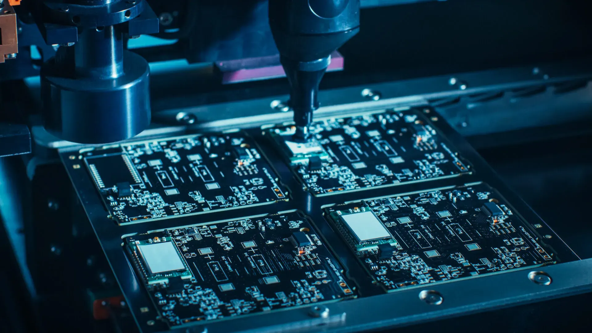
Advanced automation incorporates machine learning for predictive maintenance, averting breakdowns that halt production and spike energy use. Servo-driven conveyors and laser-guided drilling reduce material removal by optimizing hole sizes to exact specifications. Solder paste inspection via 3D scanners ensures uniform deposition, cutting defects from bridging or insufficient volume. These green PCB automation technologies extend to additive manufacturing hybrids, where selective deposition layers materials precisely, slashing chemical waste from subtractive etching.
Thermal management in reflow ovens benefits from zoned heating controlled by automation, minimizing preheat and peak temperatures. Nitrogen atmospheres, automated for purity, lower oxidation risks and flux residues. Data analytics platforms aggregate runtime metrics, identifying inefficiencies like suboptimal feeder setups. Engineers appreciate how these integrate with design files for direct translation to production, fostering minimizing energy consumption in PCB production. Integration with IoT enables remote monitoring, further trimming operational overhead.
Selective soldering stations exemplify targeted application, applying heat only where needed versus full-wave immersion. This preserves board integrity and reduces dross generation. Collaborative robots, or cobots, handle auxiliary tasks like stencil cleaning, enhancing throughput without expanding footprints.
Best Practices for Reducing Waste in PCB Manufacturing
Start with design for manufacturability (DFM) reviews that leverage automation capabilities, optimizing panelization to maximize yield per sheet. Automated nesting algorithms fit boards tightly, trimming copper foil waste. Implement just-in-time inventory via robotic storage, preventing overstocking of reels and pastes that expire. Regular calibration of nozzles and cameras upholds precision, as per IPC guidelines for assembly acceptability. These steps form the core of reducing waste in PCB manufacturing.
Water recycling loops, monitored by sensors, recapture rinse fluids for reuse in plating baths. Automated chemical dosing maintains concentrations, avoiding dumps from imbalances. Energy audits guide upgrades to variable-frequency drives on pumps and fans. Sustainable PCB assembly practices include modular fixturing that adapts across jobs, amortizing setup costs. Factories report streamlined flows when automation syncs with enterprise systems for order batching.
Train operators on hybrid workflows where humans oversee automation, focusing on exceptions. Standardize feeders across lines to reuse setups, cutting changeover waste. Endpoint testing with flying probes verifies functionality without fixtures, saving disposables.
Minimizing Energy Consumption in PCB Production
Profile equipment loads to right-size automation cells, matching capacity to demand volumes. Regenerative braking in robotic arms recaptures motion energy, feeding back to the grid. LED lighting and HVAC tied to occupancy sensors complement process efficiencies. Green PCB automation technologies shine in low-power vision systems that process images locally, bypassing cloud latency and data centers.
Shift to lead-free solders demands precise profiling, which automation excels at through closed-loop temperature control. This complies with environmental directives while stabilizing energy profiles. Integrate solar-assisted preheaters where feasible, buffering peak grid draws. Long-term, firmware updates refine algorithms for evolving efficiencies.
Challenges and Factory Insights in Sustainable Implementation
Scaling automation requires upfront investment, but return comes via sustained savings. Compatibility between legacy designs and new systems demands iterative testing. Supply chain volatility affects feeder stocking, necessitating agile reprogramming. Factory insights highlight phased rollouts, starting with high-volume lines for quickest ROI. ISO 14001 frameworks guide continual improvement, tracking metrics like kilowatt-hours per board.
Interfacing with upstream CAD ensures automation ingests native data, avoiding translation errors. Dust control in dry processes prevents sensor fouling, maintaining uptime.
Conclusion
PCB automation redefines manufacturing by embedding sustainability into core operations. From precision waste reduction to energy-smart controls, eco-friendly practices yield measurable gains. Electric engineers play a pivotal role by designing for automated flows, amplifying these benefits. Adopting green PCB automation technologies positions the industry for regulatory compliance and resource stewardship. Ultimately, sustainable PCB assembly practices secure a viable future for electronics production.
FAQs
Q1: What is eco-friendly PCB automation?
A1: Eco-friendly PCB automation employs robotic systems, AI-driven inspection, and optimized software to minimize resource use in production. It targets precision placement and real-time monitoring to cut defects and scrap. Factories integrate these for lower chemical and energy footprints, aligning with environmental management standards. This approach supports scalable green manufacturing without sacrificing throughput.
Q2: How does automation help in reducing waste in PCB manufacturing?
A2: Automation achieves micron accuracy in drilling, placement, and etching, slashing material overuse and rework. Vision systems detect flaws instantly, preventing propagation to later stages. Optimized panelization maximizes sheet utilization, minimizing trim scrap. These factory-driven methods transform waste streams into recyclable outputs, enhancing overall efficiency.
Q3: What are sustainable PCB assembly practices?
A3: Sustainable PCB assembly practices include lead-free processes, water recycling, and energy-efficient reflow zoning under automation control. Modular tooling reduces setup waste, while predictive maintenance avoids downtime energy spikes. Lean principles eliminate overproduction, focusing on demand-driven runs. These align quality with ecological goals for enduring viability.
Q4: How can manufacturers minimize energy consumption in PCB production?
A4: Minimize energy by profiling automation for variable speeds and regenerative systems in robots. Zone-controlled ovens apply heat selectively, cutting cycle times. IoT monitoring flags inefficiencies promptly. Material optimization upstream reduces processing loads, compounding savings across the line.
References
ISO 14001:2015 — Environmental management systems — Requirements with guidance for use. ISO, 2015
IPC-6012E — Qualification and Performance Specification for Rigid Printed Boards. IPC, 2017
IPC-A-600K — Acceptability of Printed Boards. IPC, 2020


