Introduction
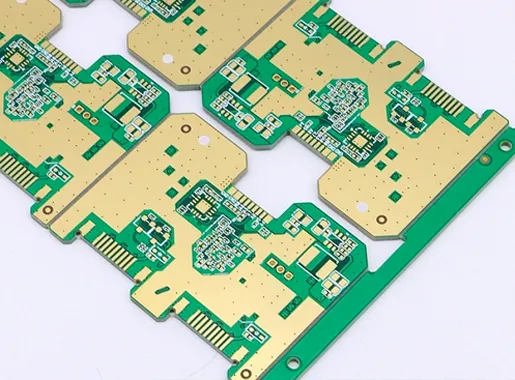
Halogen-free PCBs have become a standard choice in modern electronics manufacturing due to environmental regulations and sustainability demands. These boards eliminate halogens like bromine and chlorine from their laminate materials, replacing them with alternative flame retardants such as phosphorus-based compounds. As high-speed designs push frequencies beyond several gigahertz, engineers must evaluate how these material changes affect signal integrity. Signal integrity issues, including distortion and attenuation, can compromise performance in applications like telecommunications and data centers. Understanding the interplay between halogen-free compositions and key parameters like dielectric constant and dissipation factor is essential for reliable high-frequency PCB design. This article explores these impacts and provides practical guidance for electric engineers.
What Are Halogen-Free PCBs and Why Do They Matter for Signal Integrity?
Halogen-free PCBs adhere to industry definitions where chlorine and bromine content is below 900 parts per million each, and total halogens under 1500 parts per million. This shift addresses concerns over toxic gas emissions during fires or recycling, aligning with global eco-standards. Traditional FR-4 laminates used brominated flame retardants, but halogen-free versions rely on different resins and fillers to achieve similar fire resistance. In high-frequency PCB design, material properties directly influence signal propagation and integrity. Engineers specify laminates per IPC-4101 specifications to ensure consistent electrical performance across batches. The relevance grows as data rates increase, where even minor variations in material characteristics can lead to failures in eye diagrams or bit error rates.
Signal integrity encompasses maintaining waveform shape, timing, and amplitude throughout the transmission line. Halogen-free materials introduce variables that can alter these aspects compared to legacy options. For instance, differences in filler content affect how signals travel through the dielectric. Moisture absorption, often higher in some halogen-free formulations, can further degrade performance over time. Engineers need this knowledge to select materials that balance environmental goals with electrical demands. Proactive consideration prevents costly respins in production.
Key Technical Principles: Dielectric Constant and Signal Loss in Halogen-Free PCBs
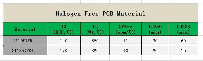
The dielectric constant, or Dk, measures a material's ability to store electrical energy in an electric field. In halogen-free PCBs, Dk values typically remain close to those of standard FR-4 but can vary based on resin chemistry and frequency. Higher Dk slows signal propagation speed, as velocity is inversely proportional to the square root of Dk. This shift impacts timing budgets in multi-gigabit designs. Engineers model these effects during stackup planning to predict delays accurately. Stability of Dk across frequencies and temperatures is crucial for consistent halogen-free PCB signal integrity.
Dissipation factor, or Df, quantifies energy loss as heat in the dielectric. Halogen-free materials sometimes exhibit higher Df than brominated counterparts, especially at microwave frequencies, leading to increased signal loss. Attenuation rises linearly with Df and frequency, following the relation alpha = (pi * f * Df * sqrt(Dk)) / (c * ln(10)/8.686), where c is the speed of light. This loss manifests as reduced eye height and increased jitter. In practice, engineers simulate insertion loss using field solvers to quantify these effects. Selecting low-Df halogen-free laminates mitigates risks in high-speed links.
Moisture absorption plays a pivotal role, as water increases both Dk and Df dynamically. Halogen-free boards may absorb more moisture due to hydrophilic fillers, exacerbating signal loss in humid environments. Qualification per IPC-6012 ensures materials withstand preconditioning without excessive degradation. Engineers bake out boards before assembly and use conformal coatings for protection. These mechanisms underscore why halogen-free transitions require thorough characterization.
Impedance Matching Challenges in Halogen-Free PCB Design
Characteristic impedance depends on trace geometry and dielectric properties via Z0 = (87 / sqrt(Dk + 1.41)) * ln(5.98 * h / (0.8 * w + t)) for microstrips. Variations in Dk from halogen-free materials demand precise stackup adjustments to hit 50-ohm or 100-ohm differentials. Manufacturing tolerances amplify mismatches if not controlled. Signal reflections from impedance discontinuities cause ringing and crosstalk. In high-frequency PCB design, tolerance stacking between layers is critical.
Halogen-free laminates can have anisotropic Dk due to glass weave orientation, complicating uniform impedance. Engineers use finer glass fabrics or spread glass to minimize this. Controlled impedance testing verifies compliance post-fabrication. Vias and transitions pose additional hurdles, as stub effects compound with material losses. Best-in-class designs employ backdrilling and blind vias. These strategies preserve halogen-free PCB signal integrity under demanding conditions.
Resin content influences surface roughness, affecting conductor losses via skin effect. Smoother copper foils pair well with low-loss dielectrics. Engineers specify reverse-treated or low-profile copper for optimal performance.
Best Practices for High-Frequency PCB Design with Halogen-Free Materials
Start with material datasheets specifying Dk and Df at operating frequencies, such as 10 GHz for mmWave apps. Cross-reference against IPC-4101 grades for halogen-free compliance. Simulate full stackups including weave effects for accurate impedance matching. Use 3D solvers to predict signal loss and crosstalk.
Optimize trace routing with length matching and serpentine patterns for skew control. Minimize vias through direct routing or embedded components. Employ ground planes for return path integrity, stitching them densely. For multilayer boards, symmetric stackups reduce warpage, which indirectly aids signal integrity.
Fabrication partners should follow JEDEC J-STD-020 guidelines for moisture sensitivity handling to prevent popcorn effects altering dielectrics. Post-assembly, thermal cycling tests validate long-term stability. Field-programmable gate arrays benefit from these practices in prototyping.
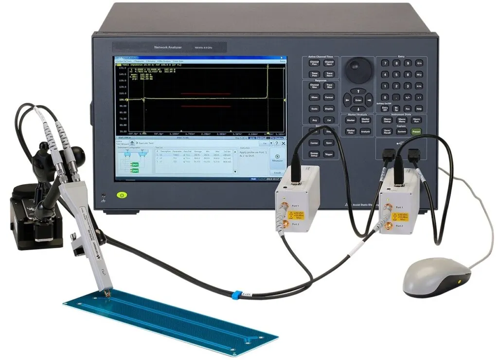
Troubleshooting common issues involves TDR measurements for impedance and VNA for S-parameters. If signal loss exceeds budgets, swap to ultra-low Df variants or thin dielectrics. Iterative simulation refines designs efficiently.
Conclusion
Halogen-free PCBs offer environmental benefits without sacrificing signal integrity when properly engineered. Key factors like dielectric constant, dissipation factor, and moisture absorption demand careful selection and design. Impedance matching and loss mitigation through stackup optimization ensure robust high-frequency performance. Adhering to standards like IPC-4101 and IPC-6012 guarantees reliability. Electric engineers equipped with these insights can navigate halogen-free transitions successfully. Future materials will further bridge any gaps, enabling sustainable high-speed electronics.
FAQs
Q1: How does halogen-free PCB signal integrity differ from traditional materials?
A1: Halogen-free boards use alternative flame retardants that can alter dielectric constant and dissipation factor, potentially increasing signal loss at high frequencies. Engineers mitigate this by selecting low-Df laminates and precise stackups. Moisture effects require handling per JEDEC J-STD-020 to maintain stability. Overall, modern formulations match or exceed legacy performance with proper design.
Q2: What role does dielectric constant play in high-frequency PCB design with halogen-free materials?
A2: Dielectric constant determines signal speed and impedance in halogen-free PCBs. Variations affect timing and reflections, critical above 5 GHz. Stable Dk across frequencies ensures predictable propagation. Engineers model per IPC-4101 specs and adjust trace widths accordingly. This preserves waveform integrity in dense layouts.
Q3: How can engineers minimize signal loss in halogen-free PCBs?
A3: Signal loss stems from higher dissipation factor in some halogen-free dielectrics. Use low-loss materials, smooth copper, and short traces. Simulate insertion loss early and employ ground shielding. Backdrilling vias reduces stubs. These steps optimize high-frequency PCB design for minimal attenuation.
Q4: Why is impedance matching vital for halogen-free PCB signal integrity?
A4: Impedance mismatches cause reflections, degrading eye quality in halogen-free designs. Dk inconsistencies demand tight stackup control. TDR verification post-fab confirms 50-ohm targets. Symmetric builds prevent warpage-induced shifts. This ensures clean signaling in multi-gigabit applications.
References
IPC-4101E — Specification for Base Materials for Rigid and Multilayer Printed Boards. IPC, 2017
IPC-6012E — Qualification and Performance Specification for Rigid Printed Boards. IPC, 2017
JEDEC J-STD-020E — Moisture/Reflow Sensitivity Classification for Nonhermetic Surface Mount Devices. JEDEC, 2014


