Introduction
PTFE PCBs play a vital role in high-frequency applications such as RF and microwave circuits, where their low dielectric constant and minimal signal loss are essential. However, assembling these boards presents unique challenges due to the material's inherent properties, including low surface energy and high coefficient of thermal expansion. Electrical engineers often encounter issues like poor solder wetting, component misalignment, and thermal stresses during reflow that can compromise reliability. Troubleshooting these problems requires a deep understanding of PTFE behavior and targeted process adjustments. This article explores common pitfalls in PTFE PCB solderability, component placement, and reflow processes, offering practical solutions to achieve robust assemblies.
Why PTFE PCB Assembly Matters
PTFE, or polytetrafluoroethylene, offers superior electrical performance in demanding environments, but its non-stick surface and thermal characteristics complicate standard surface-mount technology workflows. Poor assembly can lead to field failures in critical systems like telecommunications and aerospace electronics. Engineers must address these issues to ensure signal integrity and long-term durability. Industry standards like IPC J-STD-001 provide guidelines for soldering requirements that apply even to specialized materials like PTFE. By mastering these challenges, teams can reduce rework and improve yield rates. Ultimately, effective troubleshooting enhances the overall performance of high-frequency designs.
Technical Principles Behind Common Issues
PTFE's low surface tension makes it highly resistant to adhesion, directly impacting solderability during assembly. This property causes solder to bead up rather than spread evenly, resulting in weak joints or non-wet opens. Additionally, the material's softness increases susceptibility to handling damage, affecting precision in component placement. During thermal cycling, PTFE exhibits expansion behavior that differs significantly from copper and typical components, leading to stresses in the reflow process. These mechanisms stem from the polymer's molecular structure, which prioritizes chemical inertness over bondability. Understanding these principles is crucial for implementing effective countermeasures.
In PTFE PCB solderability, the challenge arises from inadequate surface activation, where untreated pads repel flux and molten solder. Component placement issues often involve warpage induced by prior processing or environmental exposure, causing pick-and-place machines to misalign parts. Reflow processes exacerbate these problems through uneven heating, which amplifies CTE mismatches and promotes delamination at interfaces. Moisture absorption in storage further worsens outcomes by creating voids during heating. Engineers should inspect boards for these precursors before assembly begins.
Troubleshooting PTFE PCB Solderability
PTFE PCB solderability failures manifest as de-wetting, where solder forms balls instead of fillets, or as incomplete wetting on pads. This occurs because the smooth, inert surface prevents proper flux activation and metal-to-metal contact. Contamination from handling or storage can compound the issue, trapping residues that inhibit flow. To diagnose, perform wetting balance tests or visual inspections under magnification for uniform coverage. Common culprits include insufficient surface preparation or incompatible fluxes designed for standard laminates.
Effective solutions start with surface treatments like plasma activation or chemical etching to roughen the PTFE at a molecular level, promoting adhesion without compromising electrical properties. Select fluxes formulated for low-energy surfaces, ensuring they activate fully during preheat. Apply finishes such as ENIG that enhance shelf life and wetting. Post-treatment, bake boards to remove moisture and verify solderability through dip tests. These steps align with IPC-A-610 criteria for acceptable solder joints, focusing on class 3 reliability for high-performance boards.
Always integrate incoming inspection to check for oxidation or fingerprints on pads, as PTFE's delicacy amplifies minor defects. Monitor stencil printing to avoid paste starvation on treated surfaces.
Challenges in PTFE PCB Component Placement
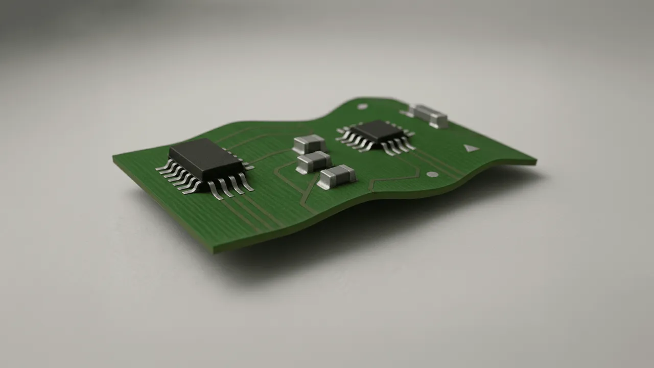
PTFE PCB component placement demands extra caution due to the material's tendency to warp under thermal or mechanical stress. Softness leads to deformation during high-force pick-and-place operations, shifting fine-pitch parts. Registration errors from fabrication carry over, misaligning fiducials and causing offsets. Humidity exposure softens the board further, exacerbating flexure. Engineers report increased tombstoning risks with small passives on uneven surfaces.
To mitigate, employ low-force nozzles and vacuum fixturing to stabilize the board during placement. Optimize machine vision for PTFE's reflective properties, adjusting lighting to capture fiducials accurately. Preheat boards gently to minimize warpage before loading. Space components per general rules, ensuring adequate clearance for reflow expansion. Pre-alignment jigs help for prototypes.
Use adhesives or tacky paste for bottom-side components to prevent movement. Verify placement accuracy with automated optical inspection post-process.
Optimizing the PTFE PCB Reflow Process
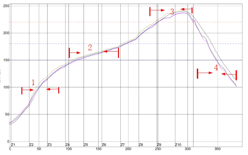
The PTFE PCB reflow process is prone to defects like bridging or opens due to aggressive expansion during peak temperatures. CTE differences cause lifting at solder joints, especially with connectors or large BGAs. Moisture trapped in the material vaporizes, forming voids or delamination. Standard profiles for FR-4 overload PTFE, leading to growth and misalignment. Profile optimization per J-STD-020 classifications is essential for moisture-sensitive levels.
Develop custom reflow curves with slower ramps and extended soaks to allow uniform heating. Prebake boards at controlled temperatures to desorb moisture without degrading the polymer. Nitrogen atmospheres reduce oxidation on pads. Monitor zone temperatures closely, adjusting conveyor speed for even exposure. Post-reflow, X-ray inspect for voids and shear test critical joints.
Incorporate conveyor supports to counter warpage, particularly for thin boards. Validate profiles with thermocouples placed at sensitive locations like vias and edges.
Best Practices for Reliable PTFE PCB Assembly
Integrate a multi-stage preparation workflow: treat surfaces, store in dry nitrogen cabinets, and process within tight windows. Train operators on gentle handling to avoid scratches that harbor contaminants. Calibrate equipment for PTFE's unique thermal response, using simulation software for profile predictions. Implement SPC to track defect rates in solderability, placement accuracy, and reflow yields.
Collaborate across design, fab, and assembly to spec stackups minimizing CTE gradients. For hybrid boards, isolate PTFE sections with hybrid prepregs. Conduct DOE on treatments to qualify plasma vs. etch efficacy.
Document lessons from failures, such as via barrel cracks from over-reflow, to refine processes.
Troubleshooting Scenarios
In one scenario, persistent de-wetting on RF connectors traced to inadequate plasma dwell time; extending exposure resolved 95% of issues. Another case involved component shifts during double-sided reflow, fixed by pallet fixturing and low-volume paste. Warped boards from storage humidity improved with vacuum baking protocols. These highlight the need for root-cause analysis using cross-sectioning and thermal profiling.
Table: Common Defects and Fixes
- Defect: Poor Solder Wetting; Likely Cause: Untreated Surface; Troubleshooting Step: Wetting Test; Fix: Plasma Etch
- Defect: Component Shift; Likely Cause: Warpage; Troubleshooting Step: Fiducial Check; Fix: Vacuum Fixture
- Defect: Voids in Joints; Likely Cause: Moisture; Troubleshooting Step: Bake Verification; Fix: Extended Prebake
- Defect: Delamination; Likely Cause: CTE Mismatch; Troubleshooting Step: Profile Audit; Fix: Slower Ramp
Conclusion
Mastering PTFE PCB assembly involves addressing solderability through surface activation, precise component placement with fixturing, and tailored reflow profiles. These practices ensure high-reliability joints in high-frequency applications. By following structured troubleshooting and standards like IPC J-STD-001 and IPC-A-610, engineers can overcome material challenges. Proactive process controls yield consistent results, reducing costs and enhancing performance. Prioritize material handling and validation for optimal outcomes.
FAQs
Q1: What causes poor PTFE PCB solderability and how to fix it?
A1: PTFE PCB solderability suffers from low surface energy, leading to beading and weak joints. Plasma treatment or chemical etching roughens the surface for better wetting. Use compatible fluxes and verify with dip tests. This aligns with soldering best practices for reliable assemblies.
Q2: How do you handle PTFE PCB component placement issues?
A2: PTFE PCB component placement challenges stem from warpage and softness, causing misalignment. Employ vacuum fixturing and low-force tools during pick-and-place. Preheat boards and use enhanced vision systems for fiducials. Post-placement AOI confirms accuracy.
Q3: What are best practices for the PTFE PCB reflow process?
A3: Optimize the PTFE PCB reflow process with custom profiles featuring slow ramps to manage expansion. Prebake to remove moisture and use nitrogen purging. Follow J-STD-020 for sensitivity classification. Monitor with thermocouples for uniform heating.
Q4: Can standard reflow ovens handle PTFE PCBs?
A4: Standard ovens work with adjustments for PTFE's thermal behavior, avoiding aggressive peaks that cause lifting. Custom curves and supports prevent warpage. Validate against assembly standards for class 3 products.
References
IPC J-STD-001 — Requirements for Soldered Electrical and Electronic Assemblies. IPC
IPC-A-610 — Acceptability of Electronic Assemblies. IPC
J-STD-020 — Moisture/Reflow Sensitivity Classification for Nonhermetic Surface Mount Devices. JEDEC


