Introduction
In the realm of printed circuit board assembly, ensuring the functionality and reliability of assembled boards stands as a cornerstone of quality control. Bed-of-nails in-circuit testing, often abbreviated as ICT, employs a specialized fixture to verify electrical performance post-assembly. This method has long been a factory staple for high-volume production, where detecting defects early prevents costly rework downstream. Electric engineers appreciate its precision in isolating issues like opens, shorts, and deviant component values. As PCB densities increase, understanding bed-of-nails testing becomes essential for optimizing design and manufacturing workflows. This article delves into its principles, implementation, and practical considerations aligned with factory-driven quality standards.
What Is Bed-of-Nails In-Circuit Testing and Why It Matters
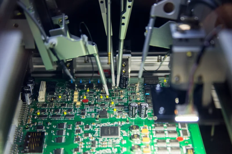
Bed-of-nails in-circuit testing refers to a technique using a custom fixture arrayed with numerous spring-loaded pins, resembling nails in a bed, to make simultaneous electrical contact with designated points on an assembled PCB. These pins press against test pads or vias, allowing the tester to inject signals and measure responses across the board's nets and components. Unlike functional testing, which evaluates the entire system, ICT focuses on individual circuits and parts in-circuit, powered at low levels to avoid damaging active devices. Factories deploy this for medium-to-high volumes because it achieves high test coverage, often exceeding 90% of nets when designed properly.
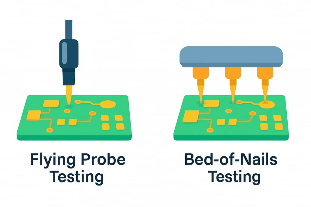
The relevance of bed-of-nails ICT lies in its ability to catch assembly defects that visual inspection misses, such as solder bridges or cold joints, ensuring compliance with quality benchmarks. In production environments, it supports rapid throughput, testing boards in seconds rather than minutes. For electric engineers, it provides granular data on component integrity, aiding root-cause analysis in failure modes. As boards evolve toward finer pitches and denser components, ICT remains vital despite alternatives like flying probes, particularly where repeatability trumps flexibility. Ultimately, integrating bed-of-nails testing into the process minimizes escapes to the field, safeguarding product reliability.

Technical Principles Behind Bed-of-Nails Testing
The core mechanism of bed-of-nails testing revolves around mechanical and electrical interfacing. The fixture aligns the PCB using tooling holes or edge clamps, then pneumatic or mechanical actuators drive the pin array upward to contact test points with controlled force, typically ensuring 50-100 grams per pin for reliable connection without board damage. Once contacted, the tester applies DC voltages, currents, or AC signals to check continuity, resistance, capacitance, inductance, and diode orientations. Guardian circuits protect against overvoltage, while software sequences tests node-by-node, comparing measurements against golden board baselines.
Electrically, the system guards against interference from parallel paths by using low-level analog measurements and digital guarding techniques. For instance, during resistor value checks, adjacent nodes are biased to minimize leakage currents. Power-up variants extend to functional sub-circuits, but standard ICT prioritizes parametric verification. Alignment precision is critical, with pin pitches often on a 2.54 mm grid to match common test point layouts. Factories calibrate fixtures regularly to maintain accuracy, as per established test method guidelines.
This setup excels in repeatability, with pin travel strokes around 1-2 mm accommodating minor board warpage. Signal integrity relies on short wiring within the fixture to reduce noise, often employing twisted pairs or coaxial cabling for high-frequency checks. Overall, these principles enable comprehensive in-circuit diagnostics, aligning with IPC-A-610 acceptability criteria for electronic assemblies.
Best Practices for Designing PCBs for Bed-of-Nails PCB Tests
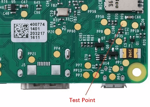
Effective bed-of-nails testing demands proactive design for testability (DFT) from the schematic stage. Engineers should provide access points as possible on every net, prioritizing unshielded nodes and avoiding hidden vias under components. Test points, typically 0.6-1.0 mm diameter pads, must offer 0.5 mm clearance from silkscreen, solder mask edges, or neighboring features to prevent shorts during probing. Place them on the same side of the board for single-sided fixtures, minimizing pin count and complexity. Tooling holes at corners, held to tight tolerances like ±0.05 mm, ensure precise registration.
Fixture design begins with CAD netlist extraction, mapping test points to pin locations while optimizing wiring lengths. Software simulates probe forces to avoid PCB flexure, especially on thin boards. Incorporate fiducials or alignment pins for automated handling in production lines. Programming involves defining test sequences, limits, and error codes, often requiring iteration based on prototype runs. Factories emphasize modular fixtures for variants, reducing redesign efforts.
Adhering to these practices maximizes coverage while mitigating common pitfalls. For instance, cluster test points on 100 mil grids to standardize pin arrays. Validate DFT through early E-test on bare boards, following IPC-9252 guidelines for electrical testing requirements. Such factory-driven approaches streamline transition to volume ICT.
Advantages and Limitations of Bed-of-Nails In-Circuit Testing
Bed-of-nails ICT shines in high-volume scenarios with its unparalleled speed, completing tests in 5-15 seconds per board, enabling thousands daily without operator fatigue. It delivers precise measurements, detecting deviations as small as 1% in passive values, and supports powered functional checks on analog sections. Repeatability stems from fixed contacts, yielding low false calls when calibrated. In factories, this translates to high uptime and data logging for process improvements.
However, notable limitations temper its universality. High initial cost arises from custom fixture fabrication, often ranging significantly based on pin count and complexity. Longer development time is required for mechanical design, wiring, and test program debugging, spanning weeks for intricate boards. The need for custom tooling and programming locks it to stable designs, ill-suited for frequent revisions. Limited test points restrict coverage in dense areas like BGAs or shielded regions, where probes cannot access inner nets without via-in-pad provisions.
Despite these, strategic use in mature production justifies the investment. Engineers weigh throughput gains against upfront expenses, often amortizing costs over 500+ units.
Practical Implementation and Troubleshooting in Factory Settings
Implementing bed-of-nails testing involves fixture procurement, test engineering, and operator training. Start with a golden board, assembled to spec, to baseline measurements. Program limits with margins for tolerance stacks, say ±5-10% for passives. In production, integrate into the line post-reflow and inspection, using vacuum hold-down for stability.
Troubleshooting common failures requires systematic isolation. Opens often trace to liftedsolder joints, verified by resistance infinity. Shorts demand pin cleaning and retest, as contamination mimics bridges. Component outliers may indicate wrong values or orientation; cross-check with hand meters. Fixture issues like bent pins or loose wiring cause intermittents, addressed via maintenance schedules.
For warpage-sensitive boards, use conformal pins or pressure distribution. Data analytics from test logs reveal trends, like yield drops signaling stencil wear. Aligning with J-STD-001 requirements for soldered assemblies ensures ICT verifies workmanship effectively.
Conclusion: Maximizing Reliability with Bed-of-Nails PCB Tests
Bed-of-nails in-circuit testing remains a robust pillar of PCB quality control, balancing speed and detail for assembled boards. By prioritizing DFT with abundant access points, engineers enable high coverage despite physical constraints. While high initial cost, longer development time, need for custom tooling and programming, and limited test points pose challenges, its factory efficiency prevails in volume runs. Integrating standards like IPC-A-610 and IPC-9252 fortifies processes against defects. Electric engineers benefit from its diagnostic depth, driving reliable products from line to application.
FAQs
Q1: What are the main limitations of bed-of-nails in-circuit testing?
A1: Bed-of-nails ICT faces high initial cost for custom fixtures, longer development time for design and programming, need for custom tooling and programming tailored to each board revision, and limited test points due to physical access requirements. These factors make it less ideal for prototypes or low-volume runs, where flying probes offer more flexibility. Factories mitigate by focusing on high-throughput designs with optimized DFT. Overall, coverage suffers in ultra-dense layouts without additional vias.
Q2: How can engineers maximize access points as possible for bed-of-nails testing?
A2: To maximize access points as possible, incorporate dedicated 1 mm test pads on all critical nets during PCB layout, ensuring 0.5 mm edge-to-edge clearance and 100 mil grid alignment. Avoid placing points under tall components or in shielded areas; use vias or breakouts for inner layers. Single-sided probing simplifies fixtures. Validate with DFT reviews early. This factory practice boosts test coverage to 95%+, aligning with IPC-9252 electrical testing guidelines.
Q3: Why does bed-of-nails testing involve longer development time?
A3: Longer development time stems from iterative fixture prototyping, pin mapping from netlists, wiring harness fabrication, and test program creation with limits and sequences. Mechanical simulations prevent alignment issues, while debug runs on prototypes refine accuracy. Unlike universal testers, each PCB variant demands bespoke tooling. Factories allocate 4-8 weeks, justified by per-unit savings in volume. Proper planning shortens cycles through standardized DFT rules.
Q4: When is bed-of-nails ICT preferable over other methods?
A4: Bed-of-nails ICT suits high-volume production needing fast, repeatable tests with limited test points optimized via DFT. Its high initial cost and need for custom tooling amortize over thousands of units, unlike slower probes for low runs. It excels verifying passives and basic functions per IPC-A-610 criteria. Choose it for stable designs prioritizing throughput in factory lines.
References
IPC-A-610H — Acceptability of Electronic Assemblies. IPC, 2019
IPC-9252 — Guidelines and Requirements for Electrical Testing of Unpopulated Printed Boards. IPC
J-STD-001H — Requirements for Soldered Electrical and Electronic Assemblies. IPC, 2018