Introduction
Thermal resistance plays a critical role in printed circuit board design, particularly as electronic devices operate under higher power densities and compact form factors. In PCBs, effective thermal management prevents overheating, which can lead to component degradation, reduced reliability, and system failures. Engineers must grasp thermal resistance to ensure heat dissipation aligns with performance requirements. This article explores PCB thermal resistance calculation, the thermal resistance of vias and PCB materials, strategies for reducing thermal resistance in PCB designs, and junction to ambient thermal resistance. By understanding these concepts, designers can optimize cooling paths and enhance overall board reliability. Key industry standards like IPC-2152 provide guidelines for thermal performance in trace design.
What Is Thermal Resistance in PCBs and Why It Matters
Thermal resistance in PCBs quantifies the opposition to heat flow, analogous to electrical resistance but for temperature gradients. Defined as θ = ΔT / Q, where ΔT is the temperature difference and Q is the heat flow rate in watts, it is expressed in Kelvin per watt (K/W) or degrees Celsius per watt (°C/W). In PCB contexts, multiple thermal resistances exist in series and parallel, forming a network from heat sources like IC junctions to ambient air. Poor thermal management increases junction temperatures, accelerating electromigration, solder joint fatigue, and dielectric breakdown. For electric engineers, mastering this metric ensures compliance with reliability targets in high-power applications such as power supplies and automotive electronics. Accurate assessment directly impacts derating factors and lifespan predictions.
The relevance intensifies with shrinking geometries and lead-free assembly processes, which elevate operating temperatures. Junction to ambient thermal resistance, often denoted θ_JA, encapsulates the total path from die to surroundings, heavily influenced by board stackup and layout. Neglecting it risks thermal runaway in densely populated boards. Standards like JEDEC JESD51 series standardize measurement conditions for comparable θ_JA values across packages and boards. Engineers prioritize this during schematic capture and layout to avoid costly respins.
Fundamental Principles of Thermal Resistance in PCBs
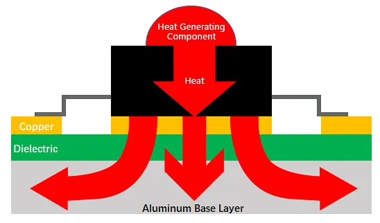
Heat transfer in PCBs occurs primarily via conduction through materials, with convection and radiation playing secondary roles at the board surface. Copper layers dominate conduction due to their high thermal conductivity, while core materials like FR4 exhibit much lower values, creating bottlenecks. The thermal resistance of PCB materials varies by composition; epoxy-based laminates conduct heat poorly in the z-direction compared to in-plane copper planes. This anisotropy necessitates careful stackup planning to channel heat laterally before vertical dissipation. Vias bridge layers, but their plated walls limit effectiveness unless filled or arrayed densely.
PCB thermal resistance calculation begins with modeling the board as a thermal network. For a simple conduction path, θ = L / (k * A), where L is path length, k is thermal conductivity, and A is cross-sectional area. Traces follow empirical models from IPC-2152, accounting for width, thickness, ambient temperature, and surrounding air effects. Multilayer boards complicate this with spreading resistance, where heat fans out from point sources. Simulation tools approximate these, but validation against standards ensures accuracy. Engineers iterate calculations early to predict hotspots.
Thermal Resistance of PCB Materials
PCB materials dictate baseline thermal performance, with copper foils providing primary pathways. Standard FR4 laminates offer thermal conductivity around 0.2 to 0.3 W/mK through-thickness, far below copper's 385 to 400 W/mK. This disparity confines heat to surface layers unless vias or embedded planes intervene. Higher-frequency or high-power laminates may incorporate fillers for improved k, but selection balances cost and signal integrity. Material CTE mismatches also induce warpage under thermal cycling, compounding resistance issues.
In multilayer designs, core and prepreg thicknesses influence vertical resistance. Thinner dielectrics reduce θ but demand finer lines. Copper weight, from 1 oz/ft2 to 6 oz/ft2, inversely scales resistance; heavier pours lower θ for power distribution. Engineers specify stackups to maximize copper fraction in heat paths. Adherence to IPC standards guides material qualification for thermal stability.
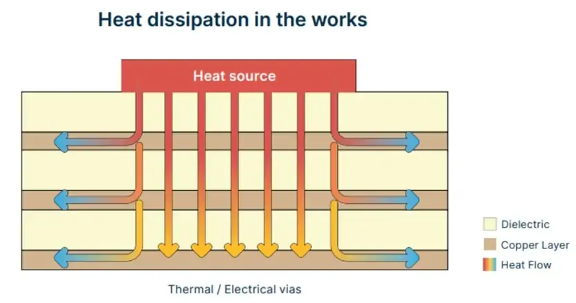
Thermal Resistance of Vias
Vias serve as vertical conduits, but their thermal resistance depends on diameter, plating thickness, and filling. A typical unfilled via has θ dominated by the thin copper barrel, often 5 to 10 K/W per via depending on length. Arrays under hot components reduce effective θ by paralleling paths. For aluminum-core applications, see our detailed guide on aluminum PCB thermal vias design rules and best practices. Filled vias, using conductive epoxy, approach solid copper performance. Placement density near pads minimizes spreading losses.
Via thermal resistance calculation treats them as cylindrical resistors: θ_via = (1/(2πk h)) * ln(r_out/r_in) for hollow, adjusted for plating. Board thickness scales resistance linearly. In high-power ICs, 20 to 50 vias per pad cut θ_JA significantly. Staggering prevents solder wicking during assembly. Optimization balances thermal gain against fabrication yield.
Junction to Ambient Thermal Resistance
Junction to ambient thermal resistance θ_JA integrates package, board, and environment contributions. JEDEC JESD51 defines test boards and conditions, like 1S0P for still air, yielding comparable metrics. Calculation decomposes into θ_JC (junction to case), θ_CS (case to board), θ_BA (board to ambient), and spreading terms. For exposed-pad packages, board vias dominate θ_CS. Typical values range widely, but design targets under 40 K/W for 1W dissipation.
θ_JA rises with board size inversely; larger areas enhance convection. Finite element analysis refines predictions, incorporating airflow. Engineers use it for power budgeting: P_max = (Tj_max - Ta_max) / θ_JA.
Best Practices for Reducing Thermal Resistance in PCB
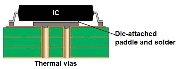
Reducing thermal resistance in PCB starts with layout: place high-power components on outer layers over solid planes. Wide traces and polygons minimize conduction θ. Power and ground planes act as heat spreaders, halving resistance versus isolated traces. Thicker copper and more layers amplify this. Learn advanced thermal pad optimization techniques for high-power components.
Incorporate thermal vias liberally under dies and pads, connecting to inner planes. Arrays of 0.3mm vias at 0.65mm pitch prove effective. Asymmetric stackups direct heat outward. Avoid silkscreen over heatsinks; expose copper for convection.
Component spacing prevents hotspot clustering. Heatsinks attach via thermal interface materials, targeting θ_SA under 10 K/W. Forced convection cuts θ_BA further. Validate with infrared thermography post-prototype. IPC-2152 charts aid trace sizing for uniform heating.
Board thickness trades off: thinner aids conduction but weakens mechanically. Multi-layer pours with stitched vias create low-θ highways. Material upgrades to metal-backed laminates suit extreme cases.
Conclusion
Mastering thermal resistance equips engineers to design robust PCBs amid rising power demands. From PCB thermal resistance calculation to optimizing vias and materials, each element contributes to lower θ_JA and reliable cooling. Implementing best practices like plane usage and via arrays yields measurable gains. Standards ensure consistency across designs. Prioritizing these metrics elevates performance while mitigating risks.
FAQs
Q1: How do you perform PCB thermal resistance calculation for traces?
A1: PCB thermal resistance calculation for traces relies on IPC-2152 charts or equations factoring current, width, thickness, and temperature rise. Input parameters into nomographs for conservative estimates, accounting for external air and board effects. Validate with simulation for multilayer spreading. This structured approach prevents overheating in power paths.
Q2: What factors influence the thermal resistance of vias?
A2: The thermal resistance of vias depends on diameter, plating thickness, length, and array density. Unfilled vias offer moderate conduction via copper walls; filling enhances it. Shorter board thickness lowers resistance linearly. Optimal pitch balances thermal performance and manufacturability in high-power designs.
Q3: What are effective ways for reducing thermal resistance in PCB?
A3: Reducing thermal resistance in PCB involves thicker copper, thermal vias under components, and solid planes for spreading. Strategic component placement avoids hotspots. Multi-layer stackups with stitched vias further improve paths. These practices align with JEDEC test conditions for verified gains.
Q4: How is junction to ambient thermal resistance determined?
A4: Junction to ambient thermal resistance measures the total heat path from die to air, per JEDEC JESD51 standards on defined boards. Decompose into package, interface, and convection terms. Calculations use θ_JA = (Tj - Ta)/P, refined by layout specifics. It guides power limits directly.
References
IPC-2152 — Standard for Determining Current Carrying Capacity in Printed Board Design. IPC, 2009
JEDEC JESD51-7 — High Effective Thermal Conductivity Test Board for Leaded Surface Mount Packages. JEDEC, 2000
IPC-2221 — Generic Standard on Printed Board Design. IPC, 2009


