Introduction
Electrical engineers constantly push the boundaries of innovation in electronics design, where time-to-market can determine project success. On-demand PCB prototyping services have emerged as a critical enabler, allowing for fast turn PCB prototypes that align production directly with design iterations. These services eliminate the delays of traditional manufacturing queues, providing boards ready for testing within days. This approach supports agile development workflows, enabling engineers to validate functionality, refine signal integrity, and optimize layouts swiftly. By leveraging on-demand capabilities, teams reduce risks associated with design flaws discovered late in the cycle. Ultimately, this manufacturing model fosters rapid innovation while maintaining adherence to established quality benchmarks.
What Is On-Demand PCB Manufacturing and Why It Matters for Prototyping
On-demand PCB manufacturing refers to a production model where printed circuit boards are fabricated in response to immediate orders, typically in low volumes for prototyping purposes. Unlike scheduled batch production, this method uses digital workflows to initiate fabrication upon file submission, minimizing setup times and inventory overhead. For electrical engineers, it matters because prototyping demands quick feedback loops to iterate on complex designs involving high-speed signals or mixed-signal circuits. Fast turn PCB prototypes from these services allow validation of electrical performance, thermal management, and mechanical fit early in development. This reduces overall project timelines and cuts costs compared to committing to full production runs prematurely. In an industry driven by shorter product lifecycles, on-demand services ensure engineers maintain momentum without compromising precision.
The relevance extends to collaborative environments where design changes occur frequently. Engineers can submit Gerber files, drill data, and stack-up specifications directly, receiving boards compliant with IPC-6012E standards for rigid printed boards. This standardization ensures prototypes mirror production intent, facilitating seamless transitions. Moreover, it democratizes access to advanced features like controlled impedance or fine-pitch traces, previously reserved for high-volume runs.
Core Technical Principles of On-Demand PCB Prototyping
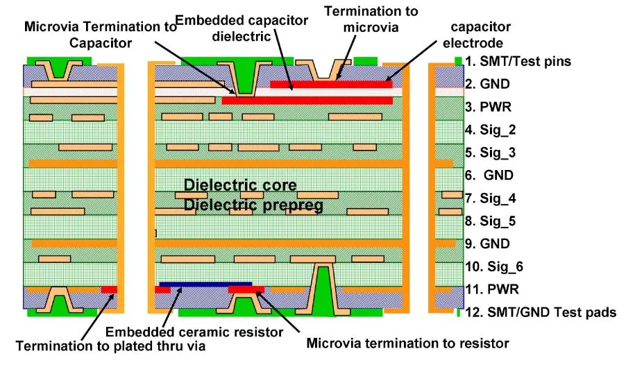
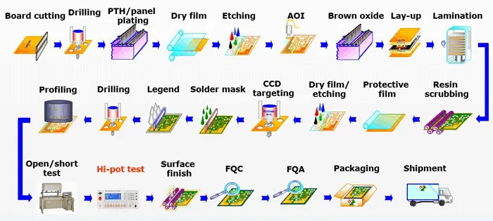
At the heart of on-demand PCB prototyping services lies a streamlined fabrication sequence optimized for speed and repeatability. The process begins with panelization, where individual designs are arrayed on larger panels to maximize material efficiency and throughput. Laser direct imaging exposes the photoresist on copper-clad laminates, defining circuit patterns with high resolution suitable for dense layouts. Chemical etching removes excess copper, followed by multi-stage desmear and plating to form vias and through-holes with precise barrel integrity.
Drilling employs high-speed CNC machines to create holes matching the specified aspect ratios, often up to 10:1 for prototypes. Solder mask application via liquid photoimageable (LPI) processes protects traces and defines pad geometries, while silkscreen adds component legends for assembly ease. Electrical testing, including flying probe for open/short detection, verifies continuity before depanelization. These steps adhere to IPC-A-600K acceptability criteria, ensuring surface finishes and plating thicknesses meet functional requirements.
Material selection plays a pivotal role, with FR-4 laminates dominating due to their balance of cost, stability, and processability. Engineers specify copper weights from 1 oz to 2 oz, dielectric thicknesses, and Tg values to suit prototype needs like high-frequency performance. Controlled impedance calculations guide trace widths and spacing, preventing signal degradation in prototypes destined for production.
PCB Design for Rapid Prototyping: Best Practices
Effective PCB design for rapid prototyping starts with manufacturability rules embedded in the layout phase. Engineers should minimize via-in-pad configurations and excessive annular ring reductions to avoid yield issues in fast turn scenarios. Panelization strategies, such as V-scoring or tab routing, optimize depanelization while preserving board integrity. Layer stack-ups must account for symmetric builds to prevent warpage, with copper balance across layers maintained within 10% variance.
Trace routing prioritizes shorter paths for high-speed signals, incorporating length matching for differential pairs. Power and ground planes should feature stitching vias to enhance thermal dissipation and EMI suppression. Design files must include complete documentation: ODB++ or Gerber RS-274X formats, IPC-D-356 netlists, and fabrication drawings specifying tolerances like ±0.1 mm for hole positions. Pre-submission DFM checks simulate processes, flagging potential issues like insufficient clearance under IPC guidelines.
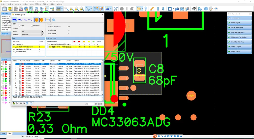
Component footprints adhere to library standards, ensuring compatibility with automated assembly. For mixed-technology boards, thermal pad designs facilitate heat transfer during reflow. Engineers benefit from simulating solder joint formation to predict defects in prototype assembly.
Streamlining PCB Prototype Assembly in On-Demand Workflows
PCB prototype assembly integrates seamlessly with on-demand fabrication, often as a turnkey service encompassing SMT and selective THT placement. Solder paste is stencil-printed with 0.1 mm precision, followed by component placement using high-speed pick-and-place machines handling 01005 sizes and BGAs. Reflow soldering profiles follow JEDEC J-STD-020E for moisture sensitivity, preventing popcorn effects in prototypes. Post-reflow inspection via automated optical systems detects bridges or tombstoning early.
For complex assemblies, glue dot dispensing secures heavy components before wave soldering. Functional testing circuits in prototypes verify power sequencing and I/O interfaces. This end-to-end approach minimizes handling damage and accelerates time to test-ready boards.
Turnkey services handle bill-of-materials sourcing, focusing on lead-free alloys compliant with J-STD-001 requirements. Engineers specify test points for in-circuit probing, ensuring prototypes support bench validation of analog and digital functions.
Overcoming Challenges in Fast Turn PCB Prototypes
One common challenge in on-demand PCB prototyping services is managing tolerances under accelerated schedules. Fine-line features below 4 mil traces demand stable imaging processes to avoid under-etching. Engineers mitigate this by widening critical nets slightly in prototypes, refining later. Thermal expansion mismatches in multilayer stacks can induce warpage; symmetric builds and low-CTE materials counteract this.
Yield variability from small lots requires robust process controls, like automated optical inspection at multiple stages. For high-density interconnects, via fill options ensure reliability without slowing turnaround. Troubleshooting focuses on root causes: impedance deviations trace to stack-up errors, while opens link to drill smear.
Case insights reveal that iterative prototyping catches 80% of issues pre-production, emphasizing early electrical testing.
Conclusion
On-demand PCB manufacturing empowers electrical engineers to unlock rapid innovation through fast turn PCB prototypes and integrated assembly. By adhering to standards like IPC-6012E, IPC-A-600K, and JEDEC J-STD-020E, these services deliver reliable boards for design validation. Best practices in PCB design for rapid prototyping ensure smooth transitions to volume production. This model not only accelerates development but also enhances precision and cost-efficiency. Engineers equipped with these capabilities stay ahead in competitive landscapes, turning concepts into functional hardware swiftly.
FAQs
Q1: What are on-demand PCB prototyping services, and how do they benefit electrical engineers?
A1: On-demand PCB prototyping services fabricate boards directly from digital files in low quantities with quick turnaround times. They benefit engineers by enabling rapid design iterations, early validation of signal integrity, and reduced time-to-market. Compliance with IPC standards ensures prototypes match production quality. This approach supports agile workflows without large upfront investments.
Q2: How fast can a fast turn PCB prototype be delivered?
A2: Fast turn PCB prototypes typically ship within 24 to 72 hours for standard designs, depending on complexity and queue. Factors like layer count and feature density influence speed, but optimized processes prioritize single-day options for 2-layer boards. Engineers gain immediate feedback for refinements. Always confirm stack-up feasibility upfront.
Q3: What role does PCB design for rapid prototyping play in on-demand services?
A3: PCB design for rapid prototyping incorporates DFM rules to maximize yield and speed, such as symmetric stack-ups and standard via sizes. It prevents delays from redesigns by simulating fabrication challenges. Engineers focus on impedance control and panelization for efficiency. This ensures prototypes function as intended post-assembly.
Q4: Why integrate PCB prototype assembly with on-demand manufacturing?
A4: Integrating PCB prototype assembly with on-demand manufacturing provides turnkey boards ready for testing, combining fabrication and population in one workflow. It minimizes handling risks and aligns reflow profiles with JEDEC guidelines. Engineers validate full functionality faster, identifying assembly issues early. This streamlines development cycles effectively.
References
IPC-6012E — Qualification and Performance Specification for Rigid Printed Boards. IPC, 2015
IPC-A-600K — Acceptability of Printed Boards. IPC, 2020
JEDEC J-STD-020E — Moisture/Reflow Sensitivity Classification of Nonhermetic Surface Mount Devices. JEDEC, 2014