Introduction
In the realm of high-speed electronics, achieving reliable performance at elevated frequencies demands materials that minimize signal degradation and maintain precise electrical characteristics. Polytetrafluoroethylene (PTFE) printed circuit boards stand out for their exceptional suitability in such demanding applications, including radar systems, telecommunications infrastructure, and satellite communications. PTFE PCB high frequency design requires careful consideration of dielectric properties to ensure optimal signal propagation. Engineers face unique challenges in manufacturing these boards due to the material's inherent traits, such as softness and thermal sensitivity. This article explores the intricacies of PTFE PCB manufacturing, focusing on signal integrity and impedance control. By understanding these aspects, designers and fabricators can unlock superior high-frequency performance.
What Is PTFE PCB and Why It Matters
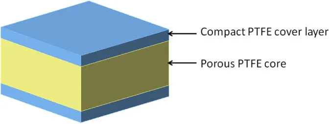
PTFE, known for its chemical inertness and thermal stability, serves as the core dielectric in high-frequency PCBs, distinguishing it from standard epoxy-based laminates. These boards leverage PTFE's low dielectric constant and dissipation factor to support signal frequencies extending into the microwave range. In PTFE PCB high frequency design, the material's properties directly influence wave velocity and attenuation, making it indispensable for applications where timing precision is critical. Factory processes must account for PTFE's hydrophobicity, which aids in low moisture absorption but complicates adhesion during lamination. The relevance grows with the proliferation of 5G networks and mmWave technologies, where even minor losses can compromise system efficiency. Adherence to IPC-4101 ensures that base materials meet rigorous qualification criteria for such environments.
PTFE PCBs matter because conventional materials falter at high frequencies due to increased dielectric losses and inconsistent impedance. Engineers prioritize them to preserve PTFE PCB signal integrity, preventing issues like crosstalk and reflections that degrade data rates. Manufacturing insights reveal that PTFE's dimensional stability under temperature variations supports reliable multilayer stackups. Without these boards, high-frequency systems would suffer from excessive power consumption and reduced range. Fabricators emphasize controlled environments to harness PTFE's benefits fully.
Technical Principles Behind PTFE PCB Performance
The foundation of PTFE PCB performance lies in its dielectric behavior, where the material exhibits minimal energy loss per cycle, crucial for maintaining signal amplitude over long traces. At high frequencies, electromagnetic waves propagate primarily through the dielectric, making PTFE's uniform permittivity essential for predictable behavior. PTFE PCB impedance control relies on this stability, as variations in dielectric thickness or composition can shift characteristic impedance, leading to mismatches. Skin effect confines currents to conductor surfaces, amplifying the need for smooth copper foils compatible with PTFE. Thermal expansion differences between PTFE and copper demand precise modeling to avoid delamination during operation.
Signal propagation in PTFE follows principles governed by Maxwell's equations, with low loss tangent ensuring phase linearity across bandwidths. PTFE PCB signal integrity benefits from reduced insertion loss, allowing higher data throughput without equalization overhead. Factory-driven analysis highlights how PTFE's non-polar nature resists frequency-dependent changes, unlike polar resins. Impedance is calculated using trace width, height, and dielectric height, with PTFE enabling tighter tolerances due to its consistency. These principles guide stackup design, where hybrid constructions blend PTFE with compatible cores for cost-effectiveness.
Dispersion effects, minimal in pure PTFE, preserve pulse fidelity in digital high-speed links. Engineers must consider radiation losses in microstrip configurations, mitigated by PTFE's low surface roughness requirements.
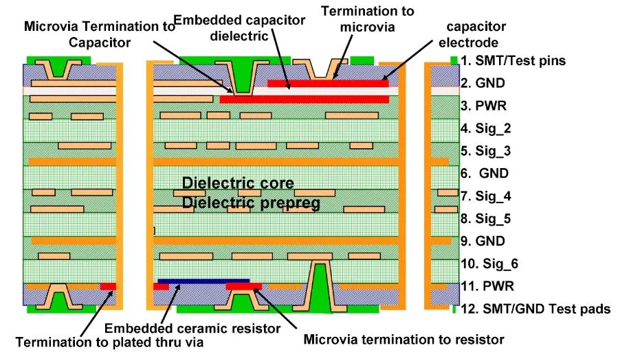
Manufacturing Process for PTFE PCBs
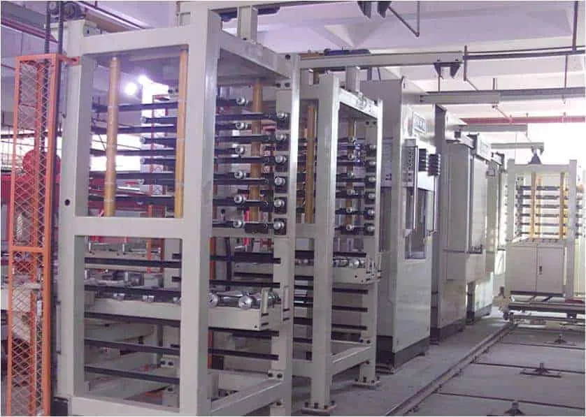
Fabricating PTFE PCBs involves specialized steps to overcome the material's softness, which complicates mechanical drilling and plating. Lamination occurs under high pressure and temperature to fuse glass-reinforced PTFE sheets with copper foil, ensuring void-free bonds. Prepreg selection per IPC-4101 slash sheets tailored for PTFE variants is critical for interlayer adhesion. Plasma treatment or chemical etching prepares surfaces for plating, addressing PTFE's low surface energy. Controlled oven curing prevents warpage, a common issue due to asymmetric CTE.
Drilling PTFE demands carbide tools at optimized speeds to minimize smear and heat buildup, followed by high-pressure desmear processes. Electroless copper deposition initiates plating, with pulse plating preferred to achieve uniform coverage on porous surfaces. Solder mask application uses low-temperature cures compatible with PTFE's melting point. Final fabrication includes contour routing with tabbing for stability. Quality checks verify thickness uniformity and electrical continuity.
Multilayer builds require sequential lamination, aligning sequential layers precisely to maintain impedance profiles. Bake-out removes residual moisture before assembly, enhancing reliability.
Best Practices for PTFE PCB High Frequency Design and Impedance Control
Successful PTFE PCB high frequency design starts with stackup optimization, balancing dielectric thickness for desired impedance while minimizing crosstalk. Use field solvers to model microstrip and stripline configurations, accounting for PTFE's anisotropy. Specify copper weights like 1 oz for reduced skin effect losses, and request low-profile foil for smoother surfaces. Tolerance calls on dielectric height should be ±10% or tighter, feasible with PTFE's processability. Factory collaboration ensures via geometries support transitions without stubs.
For PTFE PCB impedance control, target 50-ohm single-ended or 100-ohm differential lines by adjusting trace geometry iteratively. Compensate for manufacturing variations with wider margins in design rules. Signal integrity simulations incorporate PTFE's frequency-stable Dk to predict eye diagrams accurately. Avoid sharp bends and maintain ground plane integrity to suppress modes.
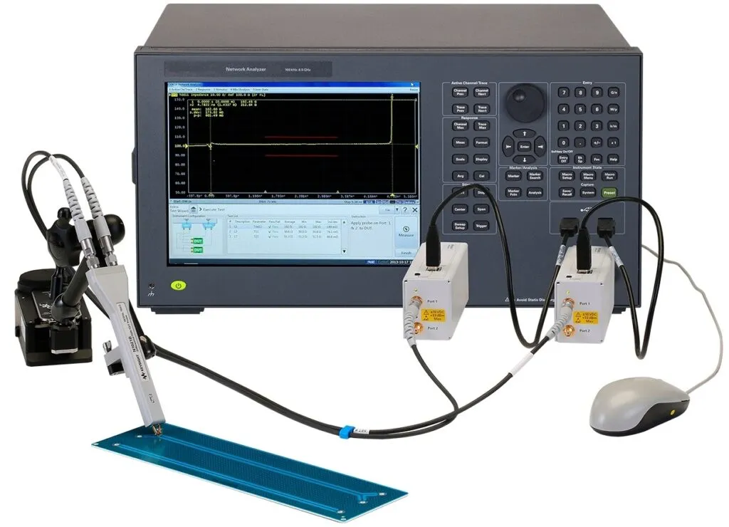
Practical troubleshooting involves thermal profiling during lamination to match CTE gradients. Post-fabrication, verify impedance with TDR measurements calibrated for PTFE velocity factor.
Hybrid stacks combining PTFE with FR4 cores reduce costs but require transition zones to manage Dk steps. Adopting IPC-6012 performance specs guarantees qualification for harsh environments.
Challenges in PTFE PCB Manufacturing and Solutions
PTFE's high CTE in the Z-axis predisposes boards to warpage during thermal cycling, necessitating symmetric stackups and fixturing. Porosity in pure PTFE invites plating voids, resolved by filled variants or extended activation cycles. Drilling wander due to softness calls for pilot holes and peck drilling sequences. Moisture, though low, affects assembly; pre-baking mitigates risks per J-STD-020 guidelines.
Signal reflections from via discontinuities challenge PTFE PCB signal integrity, addressed by back-drilling or blind vias. Cost escalations from specialized tooling demand volume planning. Factory insights stress cleanroom protocols to prevent contamination on tacky surfaces.
Conclusion
PTFE PCB manufacturing unlocks high-frequency performance through meticulous control of dielectric properties and processes. Key to success are precise impedance control and signal integrity preservation, enabled by the material's inherent low-loss nature. Engineers benefit from standard-aligned practices that ensure reliability in demanding applications. By integrating factory-driven best practices, designs achieve optimal throughput and minimal attenuation. Future advancements will further refine PTFE formulations for even higher frequencies.
FAQs
Q1: What key factors influence PTFE PCB high frequency design?
A1: PTFE PCB high frequency design hinges on dielectric constant uniformity and low dissipation for minimal signal attenuation. Stackup planning must optimize trace spacing to control crosstalk, while copper surface finish affects skin effect losses. Manufacturing tolerances on dielectric thickness directly impact performance, requiring close fabricator input. Standards like IPC-4101 guide material selection for consistency.
Q2: How does PTFE enhance PCB signal integrity?
A2: PTFE excels in PTFE PCB signal integrity by offering exceptionally low loss tangent, preserving signal amplitude across wide bandwidths. Its stable permittivity reduces phase distortion in high-speed links. Factory processes ensure void-free laminates to prevent localized losses. Designers verify integrity through simulations tailored to PTFE properties.
Q3: What are best practices for PTFE PCB impedance control?
A3: Achieve PTFE PCB impedance control by specifying precise dielectric heights and using low-profile copper. Model with 3D solvers accounting for PTFE's properties, and apply tight fab tolerances. Post-etch verification confirms targets. Sequential lamination maintains uniformity in multilayers.
Q4: Why is specialized manufacturing needed for PTFE PCBs?
A4: PTFE's softness and thermal traits demand unique drilling, plating, and lamination techniques. High-pressure bonding and desmear processes prevent defects. Clean environments and CTE-matched builds ensure reliability, aligning with IPC-6012 for qualification.
References
IPC-4101E — Specification for Base Materials for Rigid and Multilayer Printed Boards. IPC, 2017
IPC-6012E — Qualification and Performance Specification for Rigid Printed Boards. IPC, 2015
IPC-6018D — Qualification and Performance Specification for High Frequency (Microwave) Printed Boards. IPC, 2020
J-STD-020E — Moisture/Reflow Sensitivity Classification for Nonhermetic Surface Mount Devices. JEDEC, 2014