Introduction
In multilayer PCB fabrication, the drilling process forms the foundation for reliable interconnections between layers. Engineers must optimize parameters to ensure precise vias and through-holes that support high-density designs without compromising signal integrity. Poor drilling leads to defects like burrs, smear, or misalignment, which affect plating and overall board performance. This article explores the PCB drilling process, focusing on drill bit selection, drilling speed and feed, and strategies for superior hole quality in PCBs. By aligning with industry standards such as IPC-DR-572A, fabricators can achieve consistent results in demanding applications. Understanding these elements empowers electric engineers to specify designs that translate seamlessly into production.
Understanding the PCB Drilling Process in Multilayer Boards
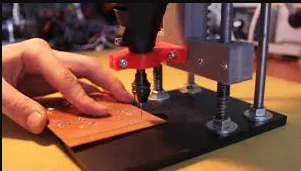
The PCB drilling process involves creating vias and through-holes after lamination to connect copper layers in multilayer stacks. Panels are typically stacked with entry and exit materials to protect surfaces and maintain alignment during high-speed CNC operations. Mechanical drilling predominates for standard vias, while laser methods handle microvias in high-density interconnects. Registration accuracy is critical, verified via X-ray before drilling to prevent layer shifts. Post-drilling steps like desmear and plating preparation directly depend on hole wall quality from the initial process. Factory-driven optimization ensures compliance with performance specifications in IPC-6012.
Multilayer boards present unique challenges due to varying thicknesses and material compositions compared to single or double-sided types. Thicker stacks require controlled depth drilling to avoid breakthrough errors, while aspect ratios influence parameter choices. Engineers evaluate stackup configurations early to pair drill sizes with via requirements. Precise tooling and parameter tuning minimize heat buildup, which can degrade epoxy resins. Consistent process control across production runs maintains yield rates and reliability.
Drill Bit Selection for Optimal Performance
Drill bit selection is pivotal in the PCB drilling process, as the wrong tool leads to rapid wear, breakage, or poor hole geometry. Carbide bits, prized for their hardness and flute design, dominate professional fabrication due to their ability to handle abrasive FR-4 materials. Micro drills suit vias under 0.45 mm, while standard bits cover larger through-holes. Bit geometry, including helix angle and web thickness, affects chip evacuation and stability in deep holes. Factory experts match bits to board thickness and layer count for extended tool life.
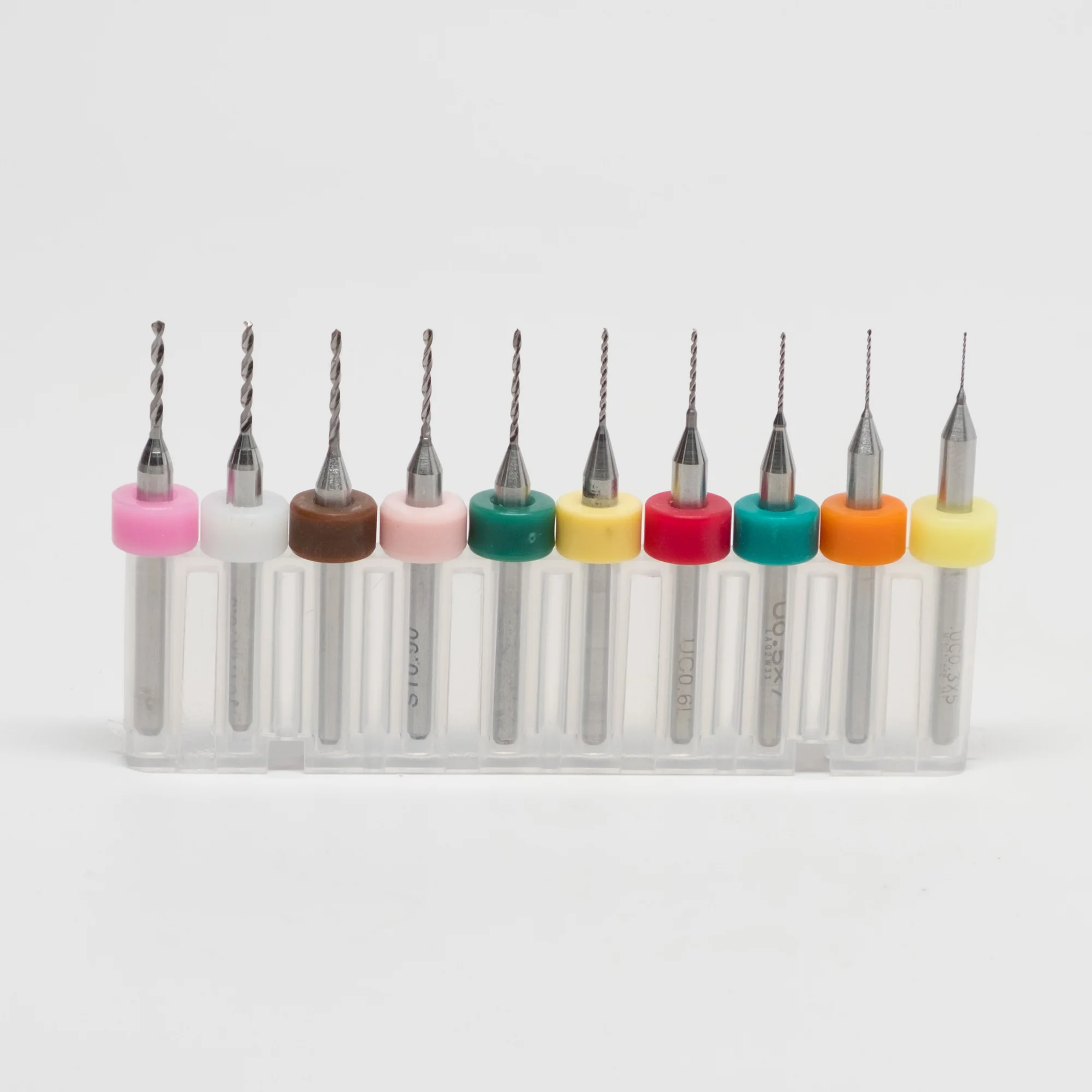
Factors like shank diameter and overall length influence machine compatibility and rigidity during high-RPM spins. Regrinding practices extend usability, but only within tolerance limits to preserve hole accuracy. Engineers specify bit types in drill files, considering tolerances defined in design rules. Selecting undercutter or straight flute designs optimizes for specific hole types in multilayer boards. Regular inspection prevents defects propagating to plating stages. Discover laser-specific parameter tuning in Optimizing Laser Drilling Parameters: A Deep Dive.
Drilling Speed and Feed: Balancing Efficiency and Quality
Drilling speed and feed rates dictate chip load, heat generation, and hole wall finish in the PCB drilling process. Spindle speeds escalate for smaller bits to maintain surface velocity, typically ranging higher for microvias to reduce torque stress. Feed rates adjust per revolution to clear debris without excessive force that causes delamination. Retract speeds prevent dwell time, minimizing smear on copper lands. Optimization balances throughput with hole quality in PCBs, guided by material properties and stack height.
Parameters vary by drill diameter and board aspect ratio, with lower feeds for high aspect ratios to avoid nail heading. Factory protocols employ peck drilling cycles for deep holes, retracting periodically for evacuation. Cooling with compressed air or mist controls temperatures during continuous runs. Engineers simulate parameters using CAM software to predict outcomes before production. Consistent tuning aligns with IPC-DR-572A guidelines for defect-free results.
Ensuring Hole Quality in PCBs
Hole quality in PCBs encompasses wall roughness, diameter tolerance, and freedom from defects like burrs or roughness. Mechanical forces during drilling can roughen surfaces, impeding plating adhesion and reliability. Standards like IPC-A-600 define acceptability criteria, including maximum allowable roughness and void limits. Cross-section analysis reveals smear or fiberglass protrusion, addressed through desmear processes. High-quality holes support uniform copper deposition for multilayer integrity.
Inspection methods include automated optical and electrical testing post-drilling. Tolerances tighten for Class 3 boards, demanding sub-micron precision in high-reliability applications. Parameter drift leads to tapered holes or oversize, failing annular ring requirements. Factory best practices integrate real-time monitoring to sustain quality across batches. Achieving these metrics directly enhances via reliability in dense designs.
Mechanical Drilling Fundamentals and Optimization
Mechanical drilling excels in multilayer PCB fabrication for through-holes and larger vias, leveraging CNC precision. Bits rotate at high speeds while advancing through stacked panels, generating chips removed by vacuum. Optimization focuses on minimizing tool wear through proper entry-exit materials and alignment pins. Peck cycles and optimized paths reduce heat, preserving laminate integrity. This method suits production volumes where cost-efficiency matters.
Challenges in multilayers include drill wander in thick stacks, mitigated by pilot holes or rigid tooling. Retract optimization prevents copper smearing on pads. Integration with back-drilling removes stubs for high-speed signals. Mechanical processes scale well for standard densities, ensuring compliance with IPC-6012 performance specs.
Laser Drilling vs Mechanical Drilling
Laser drilling vs mechanical drilling represents a key choice in advanced multilayer PCBs, each with distinct advantages. Mechanical suits larger diameters and through-holes, offering cost-effective throughput but limited by bit breakage below 0.10 mm. Laser ablation vaporizes material contactlessly, ideal for blind microvias in HDI boards with superior positional accuracy. However, lasers introduce heat-affected zones, requiring parameter tuning to avoid resin charring. For specialized techniques on glass-reinforced materials, explore our Ultimate Guide to Drilling Glass-Reinforced PCBs.
Mechanical drilling handles thicker boards better, while lasers excel in aspect ratios over 1:1 for tiny features. Hybrid approaches combine both for optimized stackups, using mechanical for press-fit holes and laser for interconnects. Electric engineers weigh density needs against fabrication costs. Laser reduces tool wear but demands desmear for carbon residue. Mechanical remains foundational, enhanced by parameter refinements.
Best Practices for Multilayer PCB Drilling
Implement panel stacking with consistent thicknesses to distribute loads evenly during drilling. Use X-ray registration for layer alignment before operations commence. Select entry films that minimize burrs and exit boards that prevent breakout. Optimize drilling speed and feed iteratively based on trial runs and tool feedback. Integrate desmear immediately post-drill to remove epoxy smear, ensuring plating readiness. Learn advanced back-drilling methods in our article on Advanced PCB Back Drilling Techniques for High-Speed Circuits.
Monitor bit life through hit counters and automated changes to prevent defect spikes. Employ controlled depth for blind vias, verifying with sectional analysis. Factory protocols include coolant systems for sustained high-RPM performance. Collaborate on design rules early to match drill capabilities with via specs. These practices align with IPC-A-600 for visual and functional acceptability.
Regular maintenance of spindles and fixtures upholds precision over long runs. Data logging enables process analytics for continuous improvement. Troubleshooting common issues like rough walls involves feed reductions or speed increases. Scaling to high-mix production requires flexible programming.
Conclusion
Optimizing drilling parameters transforms the PCB drilling process from routine to precision engineering. Drill bit selection, drilling speed and feed, and method choices directly impact hole quality in PCBs. Mechanical drilling provides robustness for multilayers, complemented by laser for micro-features. Adhering to standards like IPC-DR-572A and IPC-6012 ensures factory reliability. Electric engineers benefit from these insights to design manufacturable boards that excel in performance. Proactive optimization drives yield and longevity in complex fabrications.
FAQs
Q1: What factors influence drill bit selection in the PCB drilling process?
A1: Drill bit selection depends on hole size, board thickness, and material abrasiveness. Carbide bits are standard for their durability in FR-4 multilayers. Micro bits handle small vias, while larger ones suit through-holes. Factory alignment with design tolerances prevents mismatches. Proper selection extends tool life and maintains hole quality in PCBs.
Q2: How do drilling speed and feed affect hole quality in PCBs?
A2: Drilling speed and feed balance chip evacuation, heat control, and wall finish. High speeds for small bits reduce torque, while controlled feeds avoid breakage or smear. Excessive feeds cause rough walls, impairing plating. Optimization per stackup ensures compliance with IPC-DR-572A guidelines. Monitoring prevents defects in multilayer production.
Q3: When should laser drilling replace mechanical drilling in multilayer PCBs?
A3: Laser drilling suits microvias under 0.15 mm and blind/buried types where mechanical bits fail. It offers precision without wear but suits lower volumes due to speed limits. Mechanical excels for larger through-holes and cost efficiency. Hybrid use optimizes HDI stackups. Evaluate based on density and aspect ratio needs.
Q4: What are common best practices for optimizing the PCB drilling process?
A4: Stack panels uniformly, verify registration with X-ray, and use peck cycles for deep holes. Tune parameters to material specs and monitor tool wear. Desmear promptly post-drill for clean walls. These steps enhance hole quality in PCBs per IPC-6012. Consistent execution boosts yield in factory settings.
References
IPC-DR-572A — Drilling Guidelines for Printed Boards. IPC, 2007
IPC-6012E — Qualification and Performance Specification for Rigid Printed Boards. IPC, 2015
IPC-A-600K — Acceptability of Printed Boards. IPC, 2020