Introduction
Polytetrafluoroethylene, or PTFE, serves as a premier material for high-frequency printed circuit boards due to its exceptional electrical properties. Engineers designing RF and microwave applications often turn to PTFE PCBs for their low dielectric constant and minimal signal loss, which are critical in sectors like telecommunications, aerospace, and defense. Selecting the appropriate PTFE PCB supplier becomes paramount when balancing stringent performance requirements with practical budget constraints. Poor supplier choices can lead to issues such as impedance mismatches or dimensional instability, compromising entire system reliability. This article explores essential factors for evaluating PTFE PCB manufacturers, focusing on quality assurance and cost optimization strategies tailored for electrical engineers.
Understanding PTFE PCBs and Their Industry Relevance
PTFE PCBs utilize polytetrafluoroethylene as the core dielectric material, prized for its dielectric constant typically around 2.1 and dissipation factor below 0.0005 at microwave frequencies. These boards excel in applications demanding high signal integrity, such as 5G base stations, radar systems, and satellite communications, where traditional FR4 materials fall short due to higher losses. The material's chemical inertness and thermal stability up to 260 degrees Celsius further enhance its suitability for harsh environments. However, PTFE's inherent softness and high coefficient of thermal expansion introduce fabrication complexities that demand specialized expertise from suppliers. Engineers must prioritize suppliers who demonstrate proficiency in handling these traits to ensure reliable performance.
The relevance of PTFE PCBs intensifies with the proliferation of millimeter-wave technologies and high-speed data transmission. In these contexts, even minor variations in material properties can degrade signal quality, leading to increased bit error rates or reduced range. Suppliers capable of maintaining tight tolerances on thickness and impedance control directly impact project success. By choosing a competent PTFE PCB supplier, teams can mitigate risks associated with material inconsistencies that plague lesser-qualified fabricators. For detailed design rules, see our Ultimate Guide to Designing PTFE PCBs for RF and Microwave Applications.
Technical Challenges in PTFE PCB Fabrication
Fabricating PTFE PCBs presents unique hurdles stemming from the material's physical characteristics. PTFE's low surface energy complicates copper adhesion, often requiring surface treatments like plasma etching or chemical etching to promote bonding. Drilling generates significant smear due to the material's softness, necessitating specialized laser drilling or plasma cleaning processes to achieve clean vias. Additionally, the high CTE mismatch between PTFE and copper layers can induce warpage during lamination and soldering, demanding precise control over press cycles and filler reinforcements in hybrid constructions.
Layer stackup design must account for these issues, incorporating glass or ceramic fillers to improve mechanical stability without compromising electrical performance. Suppliers should employ advanced lamination techniques, such as vacuum pressing, to minimize voids and ensure uniform resin flow. Post-fabrication inspections for bow and twist become essential, as excessive warpage exceeds allowable limits in high-frequency assemblies. Engineers benefit from suppliers who document these processes transparently, allowing for design adjustments early in the prototyping phase.
Impedance control poses another critical challenge, given PTFE's sensitivity to manufacturing variations. Trace width tolerances tighter than standard FR4 processes, often below 10 percent, require precise photolithography and etching controls. Environmental factors during fabrication, like humidity fluctuations, can alter dielectric properties, underscoring the need for controlled cleanroom environments. A reliable PTFE PCB supplier integrates these elements into their workflow, providing traceability from raw material to finished board.
Key Quality Considerations for PTFE PCB Suppliers
When evaluating PTFE PCB manufacturers, start with their material sourcing and qualification procedures. Suppliers must verify incoming laminates for consistency in dielectric constant and thickness, rejecting batches with deviations that could skew performance. Factory-driven insights reveal that pure PTFE demands fillers like silica or glass for dimensional stability, and top suppliers specify these compositions clearly in quotations.
Fabrication capabilities form the next pillar of quality assessment. Look for expertise in handling PTFE-specific processes, including sequential lamination for multilayer boards and controlled depth drilling. Compliance with IPC-6018, the qualification specification for high-frequency and microwave printed boards, ensures that suppliers meet rigorous performance criteria for PTFE constructions. This standard outlines requirements for electrical testing, mechanical integrity, and environmental withstand, providing a benchmark for supplier audits.
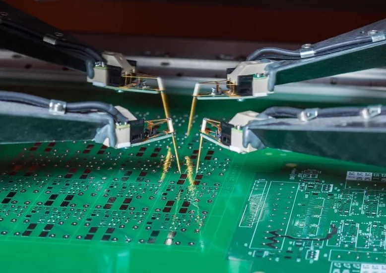
Quality control extends to in-process and final inspections. Visual and automated optical checks per IPC-A-600 acceptability criteria identify defects like delamination or plating voids early. Electrical tests, including time-domain reflectometry for impedance and vector network analysis for insertion loss, validate high-frequency performance. Certifications like ISO 9001:2015 signal a commitment to systematic quality management, reducing variability across production runs. Learn more about validation methods in our article on Testing and Validation of PTFE PCBs.
Supplier responsiveness to design feedback and prototyping turnaround times further indicates quality orientation. Engineers should request process capability indices, such as Cpk values for critical dimensions, to gauge manufacturing precision. Those demonstrating low defect rates and rework minimization deliver boards ready for assembly without additional yield losses.
Factors Influencing PTFE PCB Fabrication Cost
PTFE PCB fabrication cost hinges on several interconnected elements, starting with raw material expenses. PTFE laminates inherently command premiums over standard epoxies due to specialized synthesis and reinforcement processes. Layer count amplifies costs, as multilayer PTFE stacks require multiple lamination cycles with interlayers to manage CTE differences effectively.
Board complexity drives additional expenses through feature densities like fine-pitch traces or blind vias. High-frequency designs often necessitate low-profile copper foils and tight impedance tolerances, increasing photofab and etching overheads. Panel utilization efficiency matters too; smaller prototypes waste more material on PTFE, elevating per-unit pricing compared to production volumes.
Processing challenges contribute significantly to PTFE PCB fabrication cost. Specialized equipment for drilling, desmear, and plating raises setup fees, while lower yields from warpage or adhesion failures inflate overall expenses. Suppliers with optimized workflows, such as automated handling systems, mitigate these through economies of scale.
Volume and lead times influence pricing dynamics. Prototype runs incur higher setup costs, whereas high-volume orders benefit from amortized tooling and bulk material discounts. Negotiating tiered pricing with a trusted PTFE PCB supplier can align costs with project phases, from validation to scale-up.
Best Practices for Selecting a PTFE PCB Supplier
Begin supplier selection with a thorough capability matrix, mapping requirements against their offerings. Request detailed process flows for PTFE handling, including adhesion promotion and warpage mitigation strategies. Conduct audits or virtual tours to verify cleanroom standards and equipment suitability for high-frequency work.
Prototype iteratively with short-lead candidates to assess real-world performance. Measure delivered boards against specs for thickness uniformity, impedance accuracy, and surface finish. Analyze cost breakdowns transparently, identifying value in quality over bare minimum pricing.
Long-term partnerships yield savings through shared design guidelines and material stocking. Collaborate on DFM reviews to preempt costly revisions. Prioritize suppliers with scalable capacity matching your roadmap, ensuring continuity amid demand fluctuations. Discover real-world reliability requirements in PTFE PCBs in Aerospace and Defense.
Conclusion
Choosing the right PTFE PCB supplier demands a balanced evaluation of quality controls and cost drivers rooted in material and process realities. By focusing on proven capabilities in IPC-compliant fabrication, rigorous testing, and efficient workflows, engineers secure high-performance boards without excessive premiums. Transparent communication and prototyping validate supplier competence, paving the way for reliable RF and microwave deployments. Ultimately, investing in a capable partner optimizes both technical outcomes and PTFE PCB fabrication cost over the product lifecycle.
FAQs
Q1: What qualifications should I look for in PTFE PCB manufacturers?
A1: Reputable PTFE PCB manufacturers maintain certifications like ISO 9001:2015 and adhere to standards such as IPC-6018 for high-frequency boards. They demonstrate expertise in PTFE-specific processes, including plasma treatment for adhesion and laser drilling to control smear. Request evidence of process controls and yield data to ensure consistency. This approach minimizes risks in demanding applications.
Q2: How does material choice impact PTFE PCB fabrication cost?
A2: PTFE inherently raises costs due to premium laminates and specialized processing needs, like reinforced fillers for stability. Factors such as layer count and fine features compound expenses through extended cycles and lower yields. Volume production offsets these via efficiencies. Selecting experienced suppliers streamlines workflows, balancing PTFE PCB fabrication cost with performance.
Q3: What testing is essential from a PTFE PCB supplier?
A3: Key tests include impedance verification via TDR, warpage measurement per IPC-A-600, and dielectric strength checks. High-frequency validation through VNA assesses insertion and return loss. Cross-section analysis confirms layer integrity. A quality PTFE PCB supplier provides comprehensive reports, enabling engineers to confirm specs before assembly.
Q4: How can engineers reduce costs without sacrificing PTFE PCB quality?
A4: Optimize designs for panel efficiency and standard stackups to leverage supplier economies. Prototype in smaller volumes initially, then scale. Partner with suppliers offering DFM feedback to avoid rework. Long-term agreements secure better pricing on PTFE materials and processes, maintaining quality per industry standards.
References
IPC-6018 — Qualification and Performance Specification for High Frequency (Microwave) Printed Boards. IPC.
IPC-A-600K — Acceptability of Printed Boards. IPC.
ISO 9001:2015 — Quality Management Systems. ISO.