Introduction
Lead-free printed circuit boards represent the standard in modern electronics manufacturing due to environmental regulations and sustainability goals. These boards use surface finishes like electroless nickel immersion gold, organic solderability preservative, immersion silver, and immersion tin to comply with restrictions on hazardous substances. Proper storage becomes critical because lead-free processes involve higher reflow temperatures, amplifying risks from environmental factors. Degradation during storage can compromise solderability, leading to assembly defects such as poor wetting or voids. This article explores lead-free PCB storage conditions, shelf life factors, and strategies to maintain quality until assembly. Factory professionals rely on these practices to minimize rework and ensure reliable performance.
Why Proper Storage Matters for Lead-Free PCBs
Lead-free PCBs face unique challenges compared to traditional tin-lead finishes because their surface treatments degrade faster under suboptimal conditions. Oxidation and moisture absorption accelerate intermetallic compound formation and laminate swelling, directly impacting solder joint integrity. In high-volume production, improper storage results in batch failures during reflow soldering, increasing costs and delays. Industry standards like IPC-1601A emphasize controlled environments to preserve board usability. Engineers must understand these risks to select appropriate storage protocols aligned with assembly timelines. Ultimately, effective storage safeguards yield and supports lean manufacturing operations.
Mechanisms of Degradation in Lead-Free PCBs
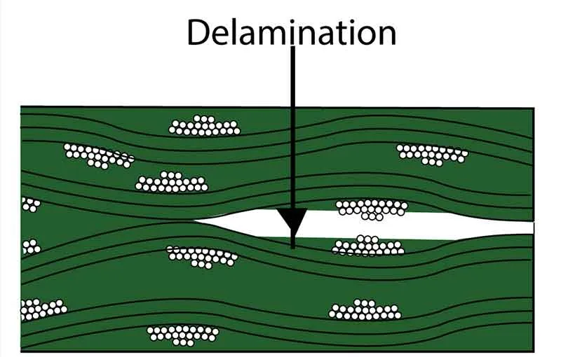
Moisture absorption in the laminate and surface finishes occurs hygroscopically, with relative humidity above 65 percent promoting rapid uptake. During lead-free reflow at 245 to 260 degrees Celsius, absorbed water vaporizes, generating internal pressure that causes delamination, blistering, or plated-through-hole cracks. Oxidation primarily affects organic and immersion finishes, where exposure to air forms oxides that hinder solder wetting. For instance, organic solderability preservative degrades into a non-conductive layer over time, reducing contact angle below acceptable thresholds. Temperature fluctuations exacerbate these issues by inducing thermal stress and warpage. These mechanisms underscore the need for proactive environmental controls in storage areas. This is especially true for OSP finishes—learn more about their strengths and limitations in our guide to exploring different finishes for FR-4 PCBs.
Recommended Lead-Free PCB Storage Conditions
IPC-1601A outlines lead-free PCB storage conditions as 15 to 30 degrees Celsius with 40 to 65 percent relative humidity for optimal preservation. These parameters minimize moisture ingress while avoiding condensation from overly low temperatures. Factory storage rooms should maintain stable conditions using HVAC systems with dehumidifiers and temperature sensors. Avoid direct sunlight and dusty areas, as ultraviolet exposure accelerates finish degradation. Vertical racking with ESD-safe separators prevents mechanical damage and particle contamination. Regular monitoring with data loggers ensures compliance, allowing early detection of excursions.
Factors Influencing Lead-Free PCB Shelf Life
Lead-free PCB shelf life varies by surface finish and packaging method, typically ranging from six to twelve months in sealed conditions per IPC-1601A guidelines. Electroless nickel immersion gold offers up to twelve months sealed, while immersion silver, immersion tin, and organic solderability preservative limit to six months due to tarnish sensitivity. Ambient storage halves these periods, necessitating immediate use or reconditioning. Board thickness and complexity also play roles, with thicker laminates absorbing more moisture over time. First-in, first-out inventory rotation extends effective usability across production lots. Engineers should label boards with fabrication dates to track against these limits. For deeper details on how surface finish choice affects long-term solderability, see our article on advanced surface finishes for PCB mass production.
- Electroless Nickel Immersion Gold: sealed shelf life up to 12 months; ambient about 6 months.
- Immersion Silver: sealed shelf life 6 to 12 months; ambient 3 to 6 months.
- Immersion Tin: sealed shelf life 6 months; ambient 3 months.
- Organic Solderability Preservative: sealed shelf life 6 months; ambient 3 months.
Lead-Free PCB Humidity Control Strategies
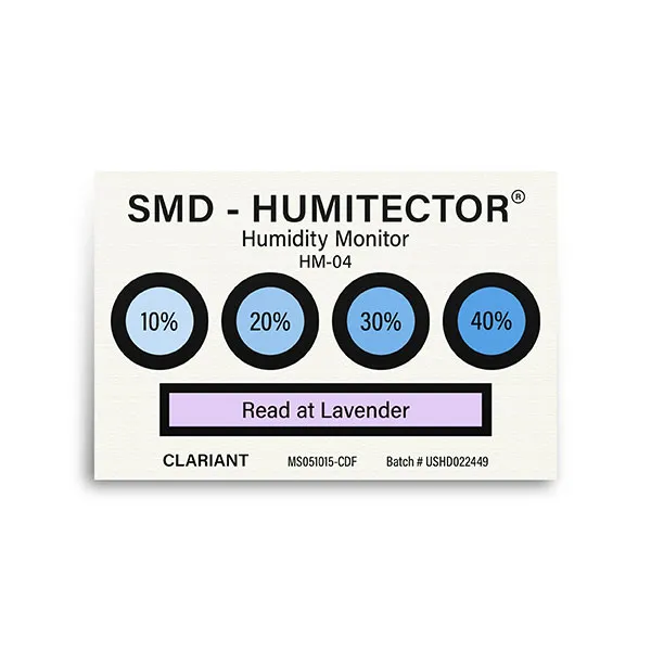
Effective lead-free PCB humidity control starts with moisture barrier bags containing desiccants and humidity indicator cards. These bags limit water vapor transmission to prevent internal relative humidity from exceeding 10 percent. Upon opening, floor life aligns with moisture sensitivity levels from related standards like J-STD-033, often 48 to 168 hours at under 60 percent relative humidity. Dry cabinets maintaining below five percent relative humidity suit high-sensitivity batches. Reseal unused boards promptly to reset the clock on shelf life. Integrating these controls into factory workflows reduces baking frequency before assembly.
Lead-Free PCB Oxidation Prevention Techniques
Oxidation prevention for lead-free PCBs requires sulfur-free, pH-neutral packaging materials, especially for immersion silver finishes prone to tarnish. Vacuum sealing removes oxygen while desiccants manage residual humidity, slowing oxide layer formation on exposed copper. Avoid baking organic solderability preservative boards, as heat above 100 degrees Celsius compromises the protective film. Stack boards with anti-static foam separators to limit air circulation between surfaces. Factory protocols should include cleanroom handling post-unpacking to prevent fingerprint oils from catalyzing oxidation. These measures align with IPC-1601A to sustain surface integrity for soldering.
Lead-Free PCB Solderability Testing Protocols
IPC J-STD-003 defines solderability testing for printed boards, using dip-and-look and solder float methods tailored to lead-free alloys like SAC305 at 255 degrees Celsius. Test coupons from production panels undergo steam aging to simulate storage exposure, followed by flux dipping and solder immersion for wetting evaluation. Acceptance requires 95 percent coverage with smooth, continuous solder fillets. Plated-through-hole float tests measure end-dip length to verify barrel fill capability. Perform testing on aged samples exceeding shelf life thresholds to qualify boards for assembly. This factory-driven verification prevents downstream defects in high-reliability applications.
Best Practices for Factory Implementation
Implement segregated storage zones for different finishes, with dedicated racks for short-shelf-life types like organic solderability preservative. Train personnel on moisture barrier bag handling, emphasizing partial air evacuation and wide heat seals. Conduct incoming inspections for packaging integrity, rejecting compromised lots. Pre-assembly baking at 105 to 125 degrees Celsius for four to twelve hours based on thickness removes absorbed moisture without degrading finishes. Integrate automated environmental monitoring with alerts for deviations. Document all processes to support audits and continuous improvement.
Troubleshooting Storage-Related Issues
Warpage from humidity gradients manifests as bow exceeding 0.75 percent, detectable via dial gauge measurements; mitigate by equilibrating boards at ambient conditions before use.[[1]](https://www.protoexpress.com/kb/ipc-1601a-pcb-handling-and-storage-guidelines)[[2]](https://pcbsync.com/ipc-1601) Poor solder wetting after storage often traces to oxidized pads; steam aging tests confirm via contact angle exceeding 60 degrees. Delamination risks rise post-baking if profiles ignore glass transition temperature; adjust dwell times accordingly. Tarnish on immersion silver appears as dark spots; source from sulfur contamination and switch packaging. Always correlate issues back to storage logs for root cause analysis. Proactive testing resolves most concerns before full production runs.
Conclusion
Mastering lead-free PCB storage conditions prevents degradation and upholds solderability in demanding assembly environments. Key elements include temperature and humidity controls per IPC-1601A, robust packaging, and routine testing via IPC J-STD-003. These practices extend shelf life, reduce rework, and align with factory efficiency goals. Engineers benefit from structured protocols that integrate monitoring and handling standards. Prioritizing these insights ensures lead-free boards deliver reliable performance from storage to solder joint. Consistent application yields cost savings and quality assurance across the supply chain.
FAQs
Q1: What are optimal lead-free PCB storage conditions?
A1: Lead-free PCB storage conditions per IPC-1601A recommend 15 to 30 degrees Celsius and 40 to 65 percent relative humidity in a stable, dust-free environment. Use ESD-safe racking and avoid sunlight to prevent warpage and contamination. Moisture barrier bags with desiccants extend protection for long-term holding. Regular logging maintains compliance and traceability.
Q2: How long is the lead-free PCB shelf life under proper storage?
A2: Lead-free PCB shelf life ranges from six to twelve months when vacuum-sealed, depending on finishes like immersion tin at six months or electroless nickel immersion gold at twelve months. Ambient conditions shorten this to three to six months. Exceeding limits requires baking and solderability verification. Factory rotation prevents expiration risks.
Q3: Why is lead-free PCB humidity control essential?
A3: Lead-free PCB humidity control prevents moisture absorption that vaporizes during high-temperature reflow, causing defects like delamination. Maintain below 65 percent relative humidity using dry cabinets or barrier bags with humidity indicator cards. This sustains laminate integrity and finish performance. Non-compliance amplifies lead-free process sensitivities.
Q4: How to perform lead-free PCB solderability testing?
A4: Lead-free PCB solderability testing follows IPC J-STD-003 with dip-and-look at 255 degrees Celsius using SAC305 solder, requiring 95 percent wetting coverage. Include steam-aged coupons and solder float for holes. Test post-storage for qualification. Results guide acceptance or reprocessing decisions.
References
IPC-1601A — Printed Board Handling and Storage Guidelines. IPC, 2016
IPC J-STD-003D — Solderability Tests for Printed Boards. IPC, 2023
J-STD-033D — Handling, Packing, Shipping and Use of Moisture/Reflow Sensitive Surface Mount Devices. JEDEC/IPC, 2018


