Introduction
Multi-layer PCBs form the foundation of nearly every modern electronic device from smartphones to industrial controllers. A multi-layer PCB contains three or more conductive copper layers separated by insulating material and interconnected through plated vias. Beginners can successfully design and order 4-layer, 6-layer, and even 8-layer boards once they understand the basic principles. This guide explains multi-layer PCB basics in simple terms and shows how to create easy multi-layer PCB designs that fabricate reliably and cost-effectively.
Why Choose Multi-Layer Instead of 2-Layer
Two-layer boards work perfectly for simple circuits, but routing becomes impossible when designs include:
- Fine-pitch ICs (0.5 mm or smaller)
- Multiple power rails (3.3 V, 5 V, 12 V)
- High-speed signals (USB, Ethernet, DDR)
- Dense component placement on both sides
A 4-layer board with solid ground and power planes instantly solves these problems while improving EMC performance and signal quality.
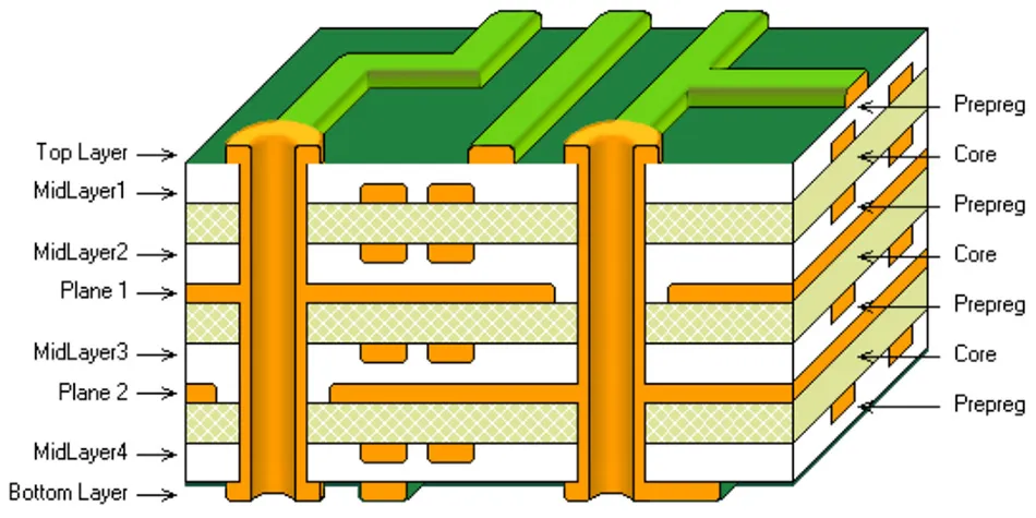
Standard Multi-Layer Stack-Ups for Beginners
4-Layer (Most Popular for Beginners)
- Layer 1: Signal (top)
- Layer 2: Ground plane (solid)
- Layer 3: Power plane (can be split)
- Layer 4: Signal (bottom)
6-Layer (Next Step)
- Layer 1: Signal
- Layer 2: Ground
- Layer 3: Signal
- Layer 4: Power
- Layer 5: Signal
- Layer 6: Ground
8-Layer (Advanced Hobby Projects)
Adds two more inner routing layers while keeping ground and power planes intact.
Simple Multi-Layer PCB Design Rules
- Keep ground and power planes completely solid when possible
- Route high-speed signals next to a reference plane (ground or power)
- Use through-hole vias for all connections (blind/buried vias increase cost)
- Place decoupling capacitors close to IC power pins
- Maintain 0.15–0.20 mm minimum trace width and spacing for hobby-friendly fabrication
- Keep total board thickness at standard values (1.6 mm for 4-layer, 1.2–1.6 mm for 6-layer)
Step-by-Step Design Process
Step 1: Schematic
Complete the full circuit diagram first. Group related components and plan power distribution.
Step 2: Component Placement
- Place connectors on board edges
- Group ICs with their decoupling capacitors
- Keep analog and digital sections separate when needed
- Leave space for routing channels
Step 3: Layer Assignment
- Route horizontal traces on top/bottom layers
- Route vertical traces on inner layers (6+ layer boards)
- Keep clock and differential pairs short and direct
Step 4: Power Distribution
- Create large power pours on the power plane
- Connect IC power pins with short, wide traces or direct vias
- Add multiple vias when connecting to planes
Step 5: Grounding
- Pour ground on all layers when possible
- Connect all ground pads directly to ground plane with vias
- Stitch ground planes together around board edges
Easy Multi-Layer PCB Fabrication Tips
- Choose 1 oz copper on outer layers and 0.5–1 oz on inner layers
- Use standard FR-4 material (Tg 130–140 °C)
- Specify ENIG or HASL surface finish
- Request electrical test on every board
- Order from fabricators who accept standard Gerber and drill files
Typical cost for 10 pieces of 100 × 100 mm 4-layer board: $30–80 including shipping.
Common Beginner Mistakes to Avoid
- Splitting ground plane into analog/digital sections (creates EMI problems)
- Routing long traces across plane gaps
- Forgetting thermal relief on plane connections
- Using too thin traces (below 0.15 mm increases cost and defects)
- Placing vias under components without solder mask dams
When to Move from 4-Layer to 6-Layer
- More than two high-speed interfaces (USB + Ethernet + HDMI)
- BGA with pitch below 0.65 mm
- Three or more different power voltages with heavy current
- Extremely dense routing that forces trace width below 0.12 mm
Conclusion
Multilayer PCB design is far more approachable than most beginners expect. Start with a clean 4-layer stack-up, maintain solid reference planes, and follow basic routing discipline. Modern fabrication capabilities make reliable the 4-layer and 6-layer board available at the same price hobbyists paid for 2-layer boards five years ago. With these fundamentals, anyone can create professional-quality multi-layer designs on their first attempt.
FAQs
Q1: How many layers should my first multi-layer PCB have?
A1: Start with 4 layers. It provides ground and power planes while keeping fabrication simple and affordable.
Q2: Is 4-layer PCB fabrication much more expensive than 2-layer?
A2: Only slightly. Most fabricators charge 2–3× the 2-layer price for small quantities of 4-layer boards.
Q3: Do I need special software for multi-layer design?
A3: No. KiCad, EasyEDA, and DesignSpark PCB all handle 4-layer and 6-layer designs perfectly for beginners.
Q4: Can I mix through-hole and SMD components on multi-layer boards?
A4: Yes, absolutely. Multi-layer construction works perfectly with both component types.
References
IPC-2221B — Generic Standard on Printed Board Design. IPC, 2015.
IPC-6012E — Qualification and Performance Specification for Rigid Printed Boards. IPC, 2017.
IPC-A-600K — Acceptability of Printed Boards. IPC, 2020.
IPC-7351B — Generic Requirements for Surface Mount Design and Land Pattern Standard. IPC, 2010.