Introduction
Fifth-generation wireless technology demands materials that support unprecedented data rates and minimal delays. PTFE PCBs emerge as a cornerstone for these requirements, particularly in high-frequency applications. Their unique properties allow signals to propagate with reduced loss, making them essential for base stations, user equipment, and network infrastructure. Engineers designing for 5G must prioritize substrates that maintain signal integrity across millimeter-wave bands. This article explores how PTFE PCBs facilitate PTFE PCB 5G antennas, PTFE PCB mmWave performance, and PTFE PCB low latency. Understanding these aspects ensures reliable deployment in demanding environments.
What Are PTFE PCBs and Why They Matter in 5G
Polytetrafluoroethylene, known as PTFE, serves as a high-performance dielectric in printed circuit boards suited for radio frequency and microwave circuits. Unlike standard epoxy-based laminates, PTFE offers exceptionally low dielectric constant and dissipation factor values, which minimize signal attenuation at frequencies above 10 GHz. In 5G networks, where sub-6 GHz and mmWave bands coexist, these characteristics prevent data bottlenecks and support massive MIMO configurations. PTFE PCB 5G antennas benefit from this material's stability, enabling compact arrays that beamform effectively without excessive power consumption. The push for low latency in applications like autonomous vehicles and industrial automation further underscores PTFE's role. Factory processes align with standards such as IPC-6018 to qualify these boards for rigorous performance.
The relevance of PTFE PCBs intensifies with 5G's spectrum allocation, extending into 24 GHz and beyond. Traditional materials suffer from higher insertion loss, degrading throughput in dense urban deployments. PTFE composites, often reinforced for manufacturability, maintain phase linearity critical for phased array antennas. Procurement teams value their thermal resilience during high-power operations. Overall, PTFE PCBs bridge the gap between theoretical speeds and practical network reliability.
Technical Principles Behind PTFE PCBs in High-Frequency 5G
PTFE's dielectric constant remains stable around 2.1 across a broad frequency range, allowing electromagnetic waves to travel faster than in higher-Dk materials. This property reduces phase velocity variations, essential for synchronizing signals in PTFE PCB mmWave systems. The low dissipation factor, typically below 0.002, converts less signal energy to heat, preserving amplitude over long traces. In 5G front-end modules, this translates to higher effective isotropic radiated power from integrated antennas. Engineers model these behaviors using field solvers to predict performance before fabrication.
Signal propagation in PTFE PCBs follows principles of minimal skin effect and dielectric loss tangent dominance at mmWave frequencies. Copper traces on PTFE exhibit lower surface roughness impact due to the material's smooth interface, further cutting conductor losses. For PTFE PCB low latency, the combined effect yields propagation delays under 1 ns per cm, aligning with 5G's URLLC requirements. Thermal expansion coefficients closer to copper than ceramics reduce stress in multilayer stacks. These mechanisms ensure that 5G signals arrive with fidelity, supporting gigabit-per-second rates.
Suggested Reading: Unlocking High Frequency Performance: A Deep Dive into PTFE PCB Manufacturing
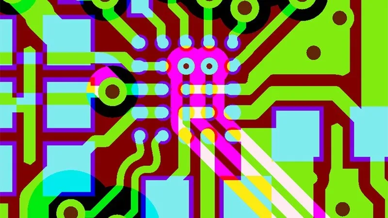
In antenna integration, PTFE substrates enable embedded patch or slot arrays directly on the board. The low-loss tangent prevents beam squint during scanning, a common issue in phased arrays. Microstrip and stripline geometries benefit from precise impedance control, often 50 ohms, maintained via filled PTFE variants. Standards like IPC-2221 guide trace width calculations to optimize return loss below -20 dB. This structured approach underpins high-speed communication in small cells and handsets.
Best Practices for Designing and Manufacturing PTFE PCBs for 5G
Selecting pure versus ceramic-filled PTFE depends on frequency and mechanical needs; filled versions offer better rigidity for multilayer builds. Design teams start with stackup simulations to balance thickness for controlled impedance in PTFE PCB 5G antennas. Sequential lamination processes mitigate warpage from CTE mismatches, adhering to factory protocols. Vias require blind or buried types with back-drilling to avoid stubs that resonate at mmWave. Controlled impedance testing post-plating verifies tolerances within 5%. For deeper RF design techniques, see our guide on designing PTFE PCBs for RF and microwave applications.
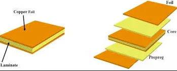
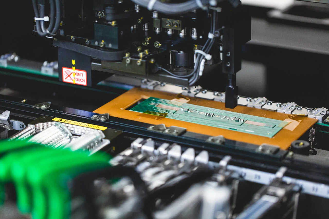
Fabrication demands specialized handling due to PTFE's low adhesion to copper foil. Plasma etching or chemical treatments pretreat surfaces for bonding, ensuring peel strength exceeds 1 N/mm. Laser drilling for high-density interconnects preserves hole wall integrity in PTFE PCB mmWave boards. Solder mask application uses low-loss overlays to shield without adding capacitance. Bake-out cycles remove absorbed moisture, preventing delamination during reflow.
Assembly guidelines emphasize low-temperature solders to avoid material degradation above 260°C. Component placement prioritizes RF paths with minimal vias, following 3W spacing rules for isolation. Testing involves vector network analyzers sweeping to 67 GHz, confirming insertion loss targets. For PTFE PCB low latency, time-domain reflectometry identifies discontinuities early. These practices, rooted in IPC-6018 qualifications, yield production-ready boards.
Troubleshooting common issues like copper drift starts with filler uniformity checks during material qualification. Warpage monitoring uses shadow moiré interferometry during cool-down. Signal integrity failures often trace to via transitions; modeling with 3D EM solvers resolves them. Field returns for excessive loss prompt dielectric constant verification via split-post resonators.
Challenges and Solutions in PTFE PCB Deployment for 5G
High costs from specialized resins challenge volume production, but hybrid stacks with FR4 cores optimize economics. Moisture absorption, though low, affects Dk stability; hermetic enclosures or conformal coatings mitigate this. Thermal management in power amplifiers requires embedded heat spreaders compatible with PTFE's expansion. Solutions include metal-filled vias for heat paths without electrical shorts.
Mechanical fragility during handling necessitates custom fixtures in factories. Reinforced glass weaves in composites enhance drillability without spiking losses. For mmWave beamforming ICs, cavity designs house dies directly on PTFE, reducing parasitics. Iterative prototyping refines these, ensuring compliance across batches.
Conclusion
PTFE PCBs stand out for enabling 5G's promises of high-speed communication and low latency through superior dielectric performance. Their integration in PTFE PCB 5G antennas and PTFE PCB mmWave circuits addresses core challenges in signal fidelity and efficiency. Best practices in design and manufacturing, guided by industry standards, ensure reliability at scale. As networks evolve, these boards will support denser deployments and emerging use cases. Engineers gain a competitive edge by mastering PTFE's nuances for next-generation wireless.
FAQs
Q1: What makes PTFE ideal for PTFE PCB 5G antennas?
A1: PTFE's low dielectric constant and dissipation factor minimize signal loss in antenna arrays, supporting efficient beamforming at sub-6 GHz and mmWave. This enables compact designs with high gain and low sidelobes. Factory processes ensure uniform properties for consistent radiation patterns. Overall, it outperforms standard laminates in throughput-critical applications.
Q2: How do PTFE PCB mmWave boards achieve low insertion loss?
A2: Low loss tangent in PTFE reduces dielectric attenuation, while smooth copper interfaces cut conductor losses above 24 GHz. Precise stackups maintain 50-ohm impedance for minimal reflections. Testing verifies performance per IPC-6018. These factors preserve signal strength in phased arrays.
Q3: Why is PTFE crucial for PTFE PCB low latency in 5G?
A3: PTFE accelerates phase velocity with its low Dk, shortening propagation times in critical paths. Reduced dissipation prevents energy loss that delays packets. This supports URLLC targets under 1 ms. Multilayer integration further optimizes latency in baseband-to-antenna links.
Q4: What standards apply to PTFE high-frequency PCBs?
A4: IPC-6018 qualifies microwave boards, specifying electrical and mechanical tests for PTFE substrates. IPC-2221 provides design guidelines for RF layouts. These ensure performance in 5G environments. Adherence minimizes field failures.
References
IPC-6018 - Qualification and Performance Specification for High Frequency (Microwave)/RF Printed Boards. IPC
IPC-2221 - Generic Standard on Printed Board Design. IPC
IPC-4101 - Specification for Base Materials for Rigid and Flexible Printed Boards. IPC