Introduction
The PCB lamination process forms the backbone of multilayer printed circuit board manufacturing, where multiple layers of copper circuits, cores, and prepregs bond into a single, robust structure. This step demands precision to ensure electrical performance, mechanical strength, and thermal reliability in demanding applications. Engineers face challenges like voids, delamination, and warpage if bonding fails, impacting signal integrity and long-term durability. Understanding the nuances of lamination pressure and temperature, along with prepreg selection, empowers design and production teams to optimize outcomes. Vacuum lamination techniques further enhance quality by minimizing defects. Mastering these elements elevates multilayer PCBs from functional boards to high-performance solutions. 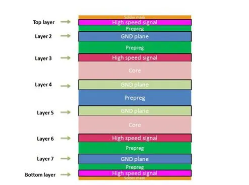
What Is the PCB Lamination Process and Why It Matters
In the PCB lamination process, inner layer cores etched with circuitry sandwich between sheets of prepreg, which act as adhesive and insulator under heat and pressure. The assembled stack enters a hydraulic press, where controlled cycles melt the prepreg resin, allowing it to flow and bond layers permanently. This creates the multilayer structure essential for complex routing in modern electronics, from telecommunications to automotive systems. Poor lamination leads to interlayer separation, compromising high-frequency performance and reliability under thermal cycling. Factory insights reveal that consistent lamination directly correlates with yield rates and field performance. Adhering to standards like IPC-4101 for base materials ensures material compatibility and process repeatability.
Multilayer PCBs rely on lamination for density and functionality that single-layer boards cannot achieve. Without perfect bonding, issues like impedance mismatches arise, critical for electric engineers designing high-speed circuits. The process influences Z-axis expansion, affecting via reliability and overall board flatness. In production, lamination sets the foundation for subsequent steps like drilling and plating. Engineers must consider stackup symmetry to balance stresses during lamination. This factory-driven approach minimizes rework and accelerates time-to-market.
Core Technical Principles of PCB Lamination
The PCB lamination process begins with meticulous layup, where operators align cores and prepregs using optical pins for registration accuracy within microns. Prepregs, partially cured B-stage epoxy sheets reinforced with glass fabric, provide the resin flow needed for bonding. Cores, fully cured laminates with copper cladding, maintain structural integrity. The stack, often 10 to 30 layers or more, undergoes preliminary pressing at low temperature to tack layers, followed by full cure in the main press. Mirror platens with release films protect the stack and ensure uniform pressure distribution. This sequence prevents shifts that could misalign traces. 
Lamination pressure and temperature control the resin's viscosity and cure kinetics. Typical cycles ramp temperature to 180 degrees C to 200 degrees C at 2 degrees C per minute, hold for 60 to 120 minutes, then cool under pressure to avoid warpage. Pressures range from 250 to 400 pounds per square inch, calibrated to prepreg flow characteristics. Excessive heat degrades resin, while insufficient pressure leaves voids. Time at temperature ensures full cross-linking for mechanical strength. Factory monitoring uses thermocouples embedded in witness panels for profile validation.
Prepreg selection for lamination hinges on resin content, flow percentage, and glass style to match stackup demands. High-flow prepregs, around 40 percent flow, suit blind vias and heavy copper, filling gaps effectively. Low-flow variants, under 10 percent, control squeeze-out in fine-pitch designs. Engineers select based on IPC-4101 specifications, considering glass transition temperature for thermal reliability. Resin content from 50 to 70 percent influences bond strength and thickness control. Matching prepreg to core CTE prevents stress-induced cracks.
Vacuum Lamination Techniques for Superior Bonding
Vacuum lamination techniques evacuate air from the press cavity, reducing trapped gases that form voids during resin flow. Full vacuum presses achieve below 10 torr, pulling bubbles from vias and between layers before cure. This method proves essential for high-layer-count boards over 20 layers, where atmospheric pressure alone risks incomplete bonding. Operators seal the stack in vacuum bags for initial de-airing, then transfer to the press. Ramp rates slow slightly under vacuum to allow thorough degassing. Results show fewer microvoids, enhancing thermal conductivity and electrical isolation.
In production, vacuum lamination pairs with low-flow prepregs to maintain line widths during squeeze. Without vacuum, air pockets expand at cure temperature, distorting traces and causing opens. Factory data indicates vacuum processes boost first-pass yields by 15 to 20 percent in complex builds. Techniques include sequential vacuum pressing for ultra-thick stacks, applying pressure incrementally. Post-lamination scanning verifies void-free cross-sections. Electric engineers appreciate this for high-reliability applications like aerospace.
Combining vacuum with optimized lamination pressure and temperature profiles minimizes oxidation risks. Nitrogen-purged environments further protect copper surfaces. Pre-baking materials at 120 degrees C for two hours removes moisture, a common void precursor. These techniques align with performance specs in IPC-6012, ensuring qualification through thermal shock and peel strength tests. Engineers simulate profiles using material datasheets for predictability.
Best Practices in Prepreg Selection and Process Control
Selecting prepregs starts with stackup analysis, balancing flow for via fill against control for impedance stability. Factory engineers review panel size, copper weights, and aspect ratios to choose styles like 1067 for thin layers or 2116 for standard. Resin systems must match core Tg, typically 170 degrees C for FR-4 grades. Over-specifying flow leads to resin starvation in dense areas. Validation involves flow tests per industry methods before full runs. This proactive selection prevents rework.
Controlled lamination pressure and temperature demand calibrated presses with multiple zones for uniformity across large panels. Profiles adjust for board thickness, with thicker stacks needing longer dwells. Cooling under full pressure to 50 degrees C locks in flatness. Process windows narrow for high-Tg materials, requiring tighter tolerances. Witness coupons track actual conditions against targets. Deviations trigger immediate adjustments. For deeper insights into stackup planning that complements these choices, read our guide on PCB Stack Up to Plan, Design, Manufacture and Repeat.
Lamination Defects and Prevention Strategies
Lamination defects like voids appear as gas pockets in cross-sections, often from moisture or rapid heating. Delamination separates layers due to weak bonds from contamination or under-cure. Warpage bows boards from asymmetric stacks or uneven cooling. IPC-A-600 criteria classify these as unacceptable for Class 2 and 3 products. Prevention starts with cleanroom handling, plasma desmear, and oxide treatments on inner layers. Ultrasonic scanning detects voids early. See how these principles apply in complex builds in our article on Multilayer PCBs in Automotive Electronics.
To prevent voids in the PCB lamination process, pre-bake all materials to below 0.25 percent moisture content. Vacuum techniques excel here, collapsing bubbles before gelation. Slow ramps allow diffusion. For delamination, ensure oxide compatibility and sufficient resin flow. Factory protocols include peel tests post-lamination, targeting 8 pounds per inch minimum.
Warpage prevention relies on symmetric stackups and matched CTE materials. Use carrier plates for thin cores during pressing. Post-cool on flat fixturing. Registration defects from layup misalignment resolve with automated pin systems and fiducials. Statistical process control tracks parameters, flagging drifts. These strategies align with IPC-6012 performance requirements, ensuring reliability under vibration and humidity.
Troubleshooting lamination defects involves root cause analysis via C-scans and microstructure. Voids cluster near vias signal ramp rate issues; adjust to 1.5 degrees C per minute. Delamination at copper-prepreg interfaces points to handling oils; implement glove policies. Warpage exceeding 0.75 percent I/100 mm triggers stack redesign. Factories log defect Pareto charts for continuous improvement. Electric engineers integrate these insights into DFM reviews.
Conclusion
Perfect layer bonding through the PCB lamination process demands expertise in prepreg selection, precise control of lamination pressure and temperature, and advanced vacuum lamination techniques. Addressing lamination defects and prevention proactively ensures multilayer PCBs meet rigorous demands. Factory-driven practices grounded in standards deliver consistent quality. Engineers gain reliability by simulating processes and validating materials upfront. Ultimately, mastering lamination transforms complex designs into dependable products, supporting innovation in electronics.
FAQs
Q1: What factors influence prepreg selection for lamination in multilayer PCBs?
A1: Prepreg selection for lamination depends on resin flow, glass style, and thickness to match stackup needs like via fill and impedance control. High-flow types suit heavy copper, while low-flow prevents squeeze-out in fine lines. Consider Tg and CTE alignment with cores per IPC-4101. Factory testing validates flow under actual pressure and temperature. This ensures strong bonding without defects.
Q2: How do lamination pressure and temperature affect multilayer PCB quality?
A2: Lamination pressure and temperature dictate resin flow and cure, typically 250 to 400 PSI and 180 to 200 degrees C. Optimal profiles minimize voids and warpage while achieving full cross-linking. Too low values leave weak bonds; excess risks degradation. Ramp and hold times tailor to prepreg specs. Monitoring via coupons maintains consistency.
Q3: What are common vacuum lamination techniques for PCBs?
A3: Vacuum lamination techniques use presses below 10 torr to remove air, ideal for high-layer counts and low-flow prepregs. Pre-vacuum bagging de-airs stacks before pressing. Nitrogen purge aids oxidation control. This prevents voids expanding at cure, boosting yields. Post-process scans verify integrity. Essential for reliable interlayer bonds.
Q4: How can engineers prevent lamination defects in the PCB lamination process?
A4: Prevent lamination defects through moisture control via pre-baking, clean handling, and symmetric stackups. Vacuum techniques eliminate voids; precise pressure and temperature profiles avoid delamination. IPC-A-600 guides acceptability. Plasma cleaning enhances adhesion. Statistical tracking identifies trends early. These steps ensure high-reliability multilayer boards.
References
IPC-4101 — Specification for Base Materials for Rigid and Multilayer Printed Boards. IPC, 2017
IPC-6012E — Qualification and Performance Specification for Rigid Printed Boards. IPC, 2018
IPC-A-600K — Acceptability of Printed Boards. IPC, 2020