Introduction
Taconic PCB lamination represents a cornerstone in high frequency PCB fabrication, enabling the creation of multilayer boards optimized for RF and microwave applications. These processes involve precise bonding of specialized laminates under controlled heat and pressure to maintain signal integrity and structural reliability. Electrical engineers rely on Taconic materials for their low loss characteristics and stability in demanding environments. Understanding the Taconic PCB lamination process ensures better design outcomes and fewer manufacturing defects. This guide delves into materials, step-by-step procedures, and factory best practices drawn from industry standards. By mastering these elements, teams can achieve superior performance in high frequency PCB fabrication.
What Is Taconic PCB Lamination and Why It Matters
Taconic PCB lamination refers to the multilayer bonding technique where pre-etched cores, prepregs, and copper foils are stacked and fused using elevated temperatures and pressures. This process forms a unified structure capable of handling high frequencies without excessive signal attenuation or distortion. In the PCB manufacturing process, lamination is pivotal for high frequency applications like radar systems and telecommunications, where material stability directly impacts performance. Poor lamination can lead to delamination, warpage, or impedance mismatches, compromising board reliability. Factory operations emphasize controlled cycles to align with material properties, ensuring compliance with qualification standards such as IPC-6012E. For electrical engineers, grasping these fundamentals optimizes designs for production scalability and cost efficiency.
The relevance stems from Taconic materials' composition, primarily PTFE reinforced with woven glass or ceramic fillers, which demand specialized handling unlike standard epoxy laminates. These materials exhibit low dielectric constants and dissipation factors, essential for minimizing insertion loss at microwave frequencies. In production, lamination precision prevents issues like resin starvation or voids, directly affecting yield rates. Engineers benefit by specifying parameters that factories can replicate reliably. Ultimately, effective Taconic PCB lamination bridges design intent with manufacturable outcomes in high frequency PCB fabrication.
Taconic PCB Materials: Key Properties and Selection
Taconic PCB materials are engineered laminates tailored for high frequency performance, featuring PTFE-based composites with ceramic fillers or woven fiberglass reinforcement. Common variants include RF-35, a ceramic-filled PTFE/glass laminate with stable dielectric properties suited for RF/multilayer hybrids; TLY-5, offering low dissipation and dimensional stability for wireless systems; and TLX series for low-profile microwave designs. These materials provide low moisture absorption, high thermal conductivity in select grades, and consistent electrical parameters across frequencies. Selection depends on dielectric constant needs, with lower Dk values like those in TLY-5 ideal for faster signal propagation.
From a factory perspective, material properties dictate lamination compatibility. Woven glass reinforcement enhances mechanical stability, reducing z-axis expansion during thermal cycles. Ceramic fillers improve thermal management without sacrificing low loss tangent values. Engineers should verify properties via test methods outlined in IPC-TM-650, ensuring alignment with application requirements. Hybrid stacks combining Taconic cores with epoxy prepregs further expand versatility while controlling costs.
Key considerations include peel strength, which relies on the dendritic structure from copper etching, and dimensional change rates typically in the 400-800 PPM range. These attributes make Taconic materials factory-friendly for high volume production when handled correctly.
Suggested Reading: Cost Effective High Frequency PCB Design: Balancing Performance and Price with Taconic Materials
The Taconic PCB Lamination Process: Step-by-Step
The Taconic PCB lamination process begins with inner layer preparation, where panels are etched and chemically cleaned to preserve surface topography for bonding. Factories acclimate materials to ambient conditions for 24 hours to minimize stress from storage variations. Copper surfaces receive oxide treatment, while PTFE faces avoid mechanical scrubbing to retain the etched dendrite imprint essential for adhesion. Stacking follows, incorporating bond plies like thermoplastic films or low-loss prepregs between cores.
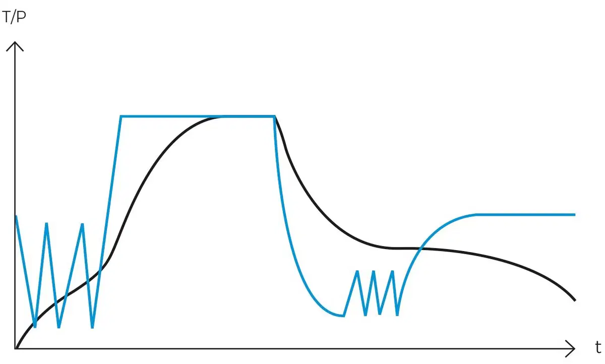
Lamination occurs in a vacuum press to eliminate voids. A typical cycle for compatible prepregs ramps temperature gradually, such as 3-10°F per minute to around 420°F, transitioning from contact to full pressure at lower thresholds like 220-230°F. Full pressure, often 400-500 psi, is maintained during the hold phase of 1 hour to allow flow and cure. Cooling under pressure prevents warpage, with rates below 6°F per minute until safe handling temperatures. For pure PTFE stacks, thermoplastic bond films like those remelting near 400°F provide low-loss interlayer dielectric.
Post-lamination, inspection per IPC-A-600 verifies bond integrity, checking for delamination or resin-rich areas. Sequential lamination suits complex builds with blind vias, repeating cycles for subsets. This controlled PCB manufacturing process ensures high frequency PCB fabrication yields boards with tight impedance control.
Best Practices for High Frequency PCB Fabrication with Taconic Laminates
Factories prioritize handling protocols to prevent distortion: lift panels by edges, use slip sheets, and avoid stacking without protection. Chemical cleaning supersedes mechanical methods, preserving bond surfaces. For drilling prior to lamination in hybrids, employ sharp carbide bits at minimum 40 psi foot pressure, followed by sodium or plasma etch for smear removal and plating activation.
Optimize press parameters per material: low ramp rates for multilayer stacks, early pressure application below melt points, and vacuum assistance for flow control. Bond ply selection, such as fastRise series for low-flow needs, ensures 4-5% resin flow without starvation. Refrigerate prepregs for handling ease.
Quality control integrates IPC-4101 for base material specs, confirming electrical stability post-lamination. Monitor warpage via dial gauge tests and perform C-scans for voids. Hybrid designs place high-frequency sections on Taconic cores, shielding with ground planes.
Troubleshoot delamination by verifying dendrite integrity and avoiding thermal excursions exceeding bond film limits. Plasma etching enhances adhesion if surfaces are compromised. These practices elevate PCB lamination reliability in production.
Suggested Reading: Designing with Taconic PCBs: A Practical Guide for RF and Microwave Engineers
Common Challenges and Troubleshooting in Taconic PCB Lamination
Warpage arises from asymmetric CTE mismatches or uneven cooling; mitigate with balanced stackups and controlled cooldowns under pressure. Voids stem from air entrapment, addressed by vacuum lamination and proper prepreg ply count. Delamination risks increase with disturbed surfaces or excessive heat; factories enforce no-scrub policies and plasma treatments.
Impedance drift post-lamination signals poor flow; adjust pressure or add plies. For high layer counts, sequential builds reduce stress. Adhering to JEDEC J-STD-020E for moisture sensitivity prevents popcorn effects in reflow.
Factory insights emphasize pilot runs for new designs, verifying via IPC-TM-650 tests.
Conclusion
Mastering Taconic PCB lamination unlocks reliable high frequency PCB fabrication through precise material handling, controlled cycles, and standard compliance. Key takeaways include chemical prep, vacuum pressing at optimized heat/pressure, and vigilant quality checks. Electrical engineers partnering with factories achieve designs that perform under extremes. Implementing these best practices minimizes defects and maximizes yield.
FAQs
Q1: What is the Taconic PCB lamination process?
A1: The Taconic PCB lamination process stacks etched cores and bond plies, then applies vacuum-assisted heat and pressure for bonding. Cycles ramp to peak temperatures around 420°F with holds for flow, followed by pressured cooling. Factories tailor parameters to material types like TLY-5 for low-loss multilayers. This ensures dimensional stability per industry practices.
Q2: How do Taconic PCB materials differ in high frequency PCB fabrication?
A2: Taconic PCB materials like RF-35 and TLY-5 feature PTFE/ceramic or glass reinforcement for low Dk/Df, outperforming epoxies in signal loss. They offer superior thermal stability and low moisture uptake, ideal for RF applications. Selection hinges on frequency and hybrid needs, with woven glass aiding mechanical robustness during lamination.
Q3: What are best practices for PCB lamination with Taconic laminates?
A3: Avoid mechanical scrubbing, use chemical cleaning, and acclimate panels pre-lamination. Employ vacuum presses with gradual ramps and full pressure holds. Inspect per IPC standards and use plasma for hole prep. These steps prevent warpage and voids in high frequency builds.
Q4: Why is pressure control critical in the Taconic PCB lamination process?
A4: Pressure ensures uniform resin flow, void elimination, and dendrite bonding in PTFE surfaces. Initial low pressure prevents squeezing out, while full loads like 500 psi cure the stack. Cooling under pressure matches CTE, reducing warpage for reliable multilayers.
References
IPC-6012E — Qualification and Performance Specification for Rigid Printed Boards. IPC, 2017
IPC-TM-650 2.5.5.5 — Test Methods Manual for Dielectric Constant Measurement. IPC, current
IPC-4101 — Specification for Base Materials for High Speed/High Frequency Applications. IPC, 2016
JEDEC J-STD-020E — Moisture/Reflow Sensitivity Classification. JEDEC, 2014