 00:54
00:54
PCB Clearance
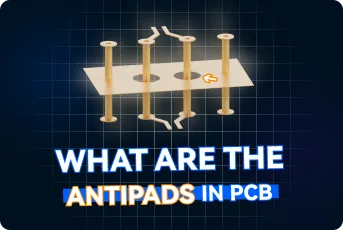
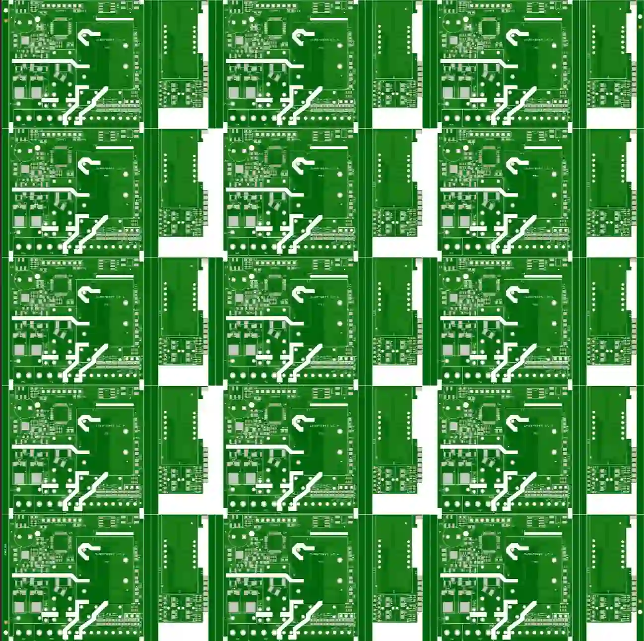
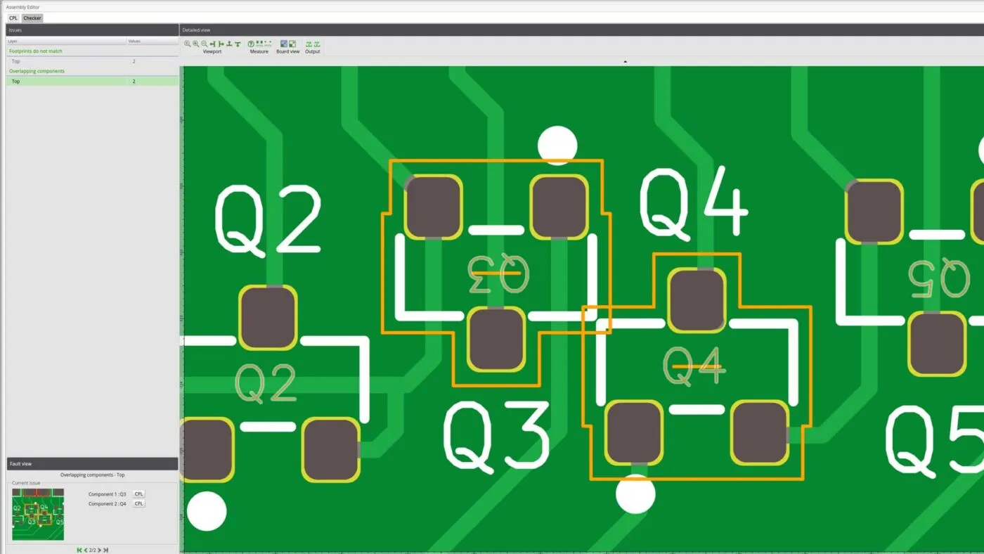
PCB clearance is a fundamental aspect of printed circuit board design that refers to the minimum distance required between conductive elements, such as traces, pads, and components, to prevent electrical breakdown, arcing, or unintended short circuits. This parameter is critical for ensuring the safety, reliability, and performance of electronic devices, particularly in applications involving high voltages or harsh environments. Engineers and designers searching for information on PCB clearance often seek guidance on adhering to industry standards like IPC-2221 or UL requirements, which dictate clearance values based on factors such as operating voltage, altitude, and pollution degrees. Understanding these guidelines helps avoid costly redesigns and failures in prototypes or production runs. In practice, calculating PCB clearance involves considering the dielectric strength of the board material, typically FR-4 or advanced substrates, alongside environmental influences like humidity and temperature. For instance, in power electronics or automotive systems, maintaining adequate clearance can prevent catastrophic failures and extend device lifespan. Best practices include using simulation tools to model electric fields and verify designs before fabrication, as well as incorporating creepage distances for added safety in contaminated settings. Designers can optimize board layouts by grouping high-voltage sections and employing conformal coatings to enhance insulation properties. Articles tagged under PCB Clearance offer detailed explorations of these topics, from beginner tutorials on basic calculations to advanced case studies in high-frequency PCB designs. By delving into these resources, you can gain practical strategies to improve your projects, whether you are troubleshooting existing boards or planning new ones for compliance and efficiency. This knowledge empowers hobbyists and professionals alike to create robust, standards-compliant electronics that perform reliably in real-world conditions.
Video Guide
-
00:54
Technical Articles
Get in Touch
Send Message
- Products & Service
- Company
- About AIVON
- Contact
- News
- Blog
- Certification
-


- Payment
-


2026 AIVON.COM All Rights Reserved