PCB Laser Drilling
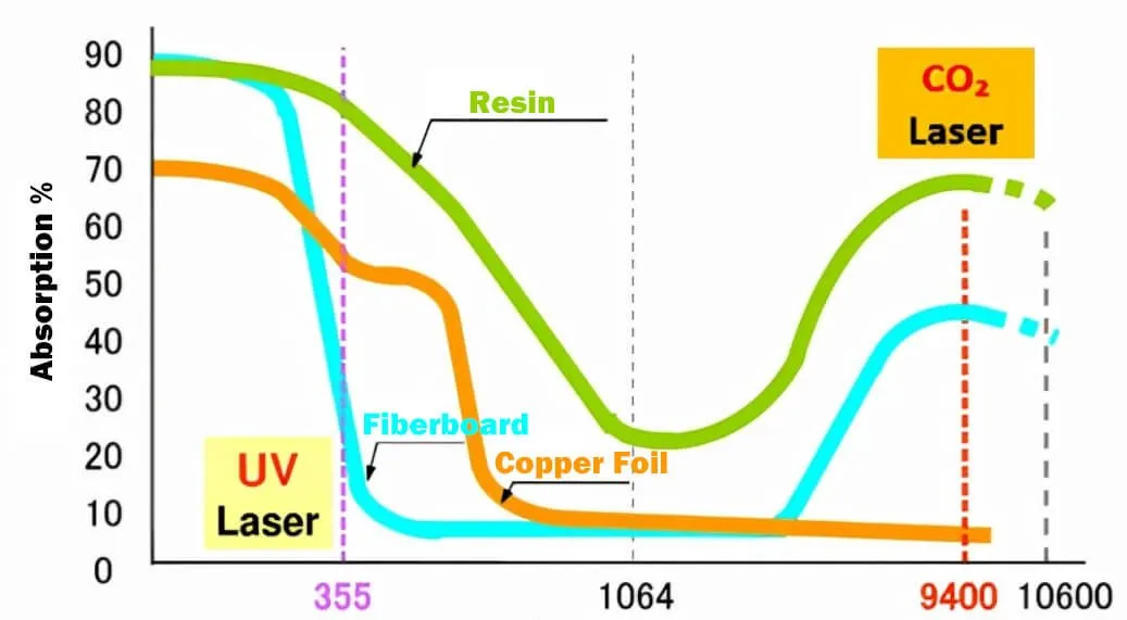
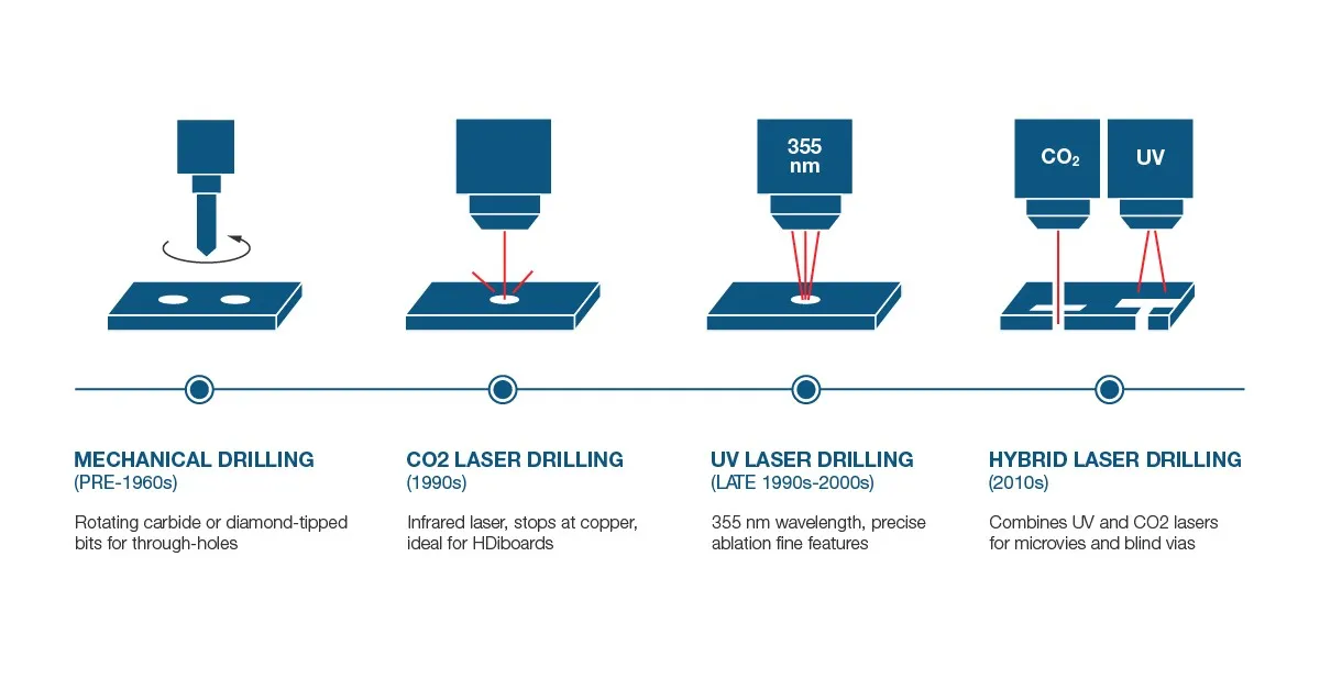
PCB laser drilling represents a cutting-edge technique in printed circuit board manufacturing, enabling the creation of precise microvias and through-holes with unparalleled accuracy. This process utilizes focused laser beams to ablate material layers, offering advantages over traditional mechanical drilling methods, such as reduced thermal damage and the ability to handle high-density interconnects. For engineers and designers searching for information on PCB laser drilling, this tag serves as a comprehensive resource, covering the fundamentals of laser types, including CO2 and UV lasers, and their suitability for various substrate materials like FR-4 or polyimide. Understanding PCB laser drilling is essential for optimizing board performance in applications where space constraints and signal integrity are critical. In industries such as consumer electronics, automotive, and telecommunications, this method facilitates the production of smaller, more reliable PCBs by allowing for blind and buried vias that enhance routing density. Practical insights include selecting appropriate laser parameters to minimize debris and ensure hole quality, as well as integrating the process into multilayer board fabrication workflows. By addressing common challenges like alignment accuracy and cost efficiency, the articles under this tag provide actionable guidance to help you achieve cleaner drills and faster production cycles. For those implementing PCB laser drilling in prototypes or volume manufacturing, best practices emphasize pre-drill inspections and post-process cleaning to prevent defects. Exploring the related content here can deepen your knowledge on integrating this technology with other PCB processes, such as etching and plating, ultimately supporting informed decisions that improve yield and reliability in your projects.
Video Guide
No videos found for this tag.
Technical Articles
Get in Touch
Send Message
- Products & Service
- Company
- About AIVON
- Contact
- News
- Blog
- Certification
-


- Payment
-


2026 AIVON.COM All Rights Reserved