 00:52
00:52
PCB Layers
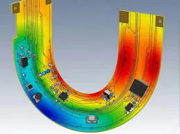
Understanding PCB layers is fundamental to designing efficient and reliable printed circuit boards, as they determine the complexity, performance, and cost of electronic assemblies. In PCB design, layers refer to the conductive copper sheets separated by insulating materials, allowing for intricate routing of signals, power, and ground planes. Single-layer PCBs are ideal for simple, low-cost applications like basic consumer gadgets, while multi-layer configurations—often ranging from four to over 20 layers—enable high-density interconnects in advanced systems such as smartphones, automotive electronics, and aerospace equipment. By exploring the PCB Layers tag, users can gain insights into how layer count influences signal integrity, electromagnetic interference reduction, and thermal management, helping to avoid common pitfalls like crosstalk or impedance mismatches. For those searching for practical guidance on PCB layers, this collection offers actionable advice on selecting the appropriate layer stackup based on project requirements. For instance, engineers can learn best practices for via placement in multi-layer boards to minimize manufacturing defects and ensure reliable soldering. Hobbyists and professionals alike will find value in discussions on cost-effective layering strategies, such as transitioning from double-sided to four-layer designs to accommodate complex circuits without excessive board size. Additionally, articles delve into advanced topics like blind and buried vias, which optimize space in compact devices. Whether you are troubleshooting layer-related issues in a prototype or planning a high-speed PCB for data centers, the resources here provide authoritative explanations grounded in industry standards. Browsing through these articles can equip you with the knowledge to enhance your designs, from initial concept to final production, ensuring robustness and efficiency in your electronic projects.
Video Guide
-
00:52
Technical Articles
Get in Touch
Send Message
- Products & Service
- Company
- About AIVON
- Contact
- News
- Blog
- Certification
-


- Payment
-


2026 AIVON.COM All Rights Reserved