Via Placement
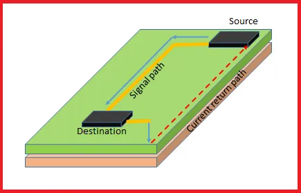
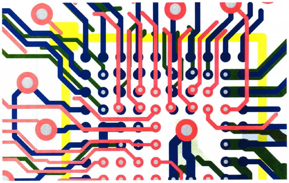
Via placement plays a critical role in printed circuit board (PCB) design, serving as the essential conduits that connect different layers of a board. These small drilled holes, filled or plated with conductive material, enable electrical signals, power, and ground to travel seamlessly between layers, ensuring the overall functionality and reliability of electronic devices. For engineers and designers searching for via placement strategies, this tag aggregates in-depth resources that address the nuances of optimizing via locations to minimize signal interference, enhance thermal dissipation, and improve manufacturing efficiency. Understanding via placement begins with recognizing its impact on high-speed circuits and dense layouts. Poorly positioned vias can lead to issues like crosstalk, impedance mismatches, or excessive heat buildup, potentially compromising the performance of everything from consumer gadgets to industrial equipment. Best practices include adhering to design rules that consider via types—such as through-hole, blind, or buried vias—and their proximity to components and traces. For instance, placing vias symmetrically around high-frequency signals can reduce electromagnetic interference, while staggering them in power planes aids in even current distribution. These techniques not only boost signal integrity but also facilitate easier prototyping and scaling in production. Professionals tackling complex PCB projects will find value in exploring the articles linked under this tag, which offer practical examples from real-world applications. Whether you are refining a multilayer board for automotive electronics or troubleshooting via-related failures in prototypes, these guides provide step-by-step insights into tools like CAD software for simulation and validation. By applying these principles, designers can achieve more robust and cost-effective PCBs, ultimately accelerating time-to-market for innovative products.
Video Guide
No videos found for this tag.
Technical Articles
Get in Touch
Send Message
- Products & Service
- Company
- About AIVON
- Contact
- News
- Blog
- Certification
-


- Payment
-


2026 AIVON.COM All Rights Reserved