-
 00:52
00:52
This PCB Hole Works without Solder | Press-fit Holes Explained
PCB press-fit holes are a solderless interconnection method used to create highly reliable electrical and mechanical connections between connectors and plated through-holes. This video explains how compliant pins are mechanically inserted into precisely manufactured holes, forming a gas-tight connection through controlled compression and spring-back against the plated barrel. It highlights key design requirements such as accurate hole sizing, strong copper plating, adequate annular rings, and strict manufacturing tolerances. The video also discusses common design risks, including insufficient contact force or barrel damage caused by incorrect hole dimensions. These guidelines are essential for ensuring robust performance in automotive, aerospace, industrial, and other high-reliability PCB applications during both prototyping and mass production.
-
 00:51
00:51
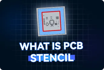
Your Soldering Problem May Start Here | PCB Stencil Selection Explained
PCB stencils play a crucial role in SMT assembly by controlling the precise amount of solder paste deposited onto component pads. This video explains how improper stencil selection can lead to defects such as solder bridging, weak joints, and open connections. It compares common stencil types, including laser-cut, electropolished, and step stencils, and discusses how stencil thickness influences paste volume, assembly quality, and first-pass yield. By understanding stencil design and selection principles, engineers can optimize solder paste printing, improve assembly reliability, and achieve better manufacturing results for HDI, consumer, medical, automotive, and other high-density PCB applications.
-
 00:53
00:53
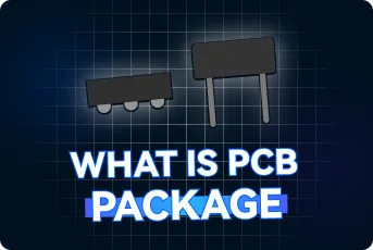
This Tiny PCB Decision Changes Everything
Component package selection is a critical PCB design decision that affects manufacturability, thermal performance, signal integrity, and long-term reliability. This video explains the differences between common package types such as QFP, QFN, and BGA, highlighting their advantages, limitations, and typical applications. It discusses important trade-offs involving component density, solder joint inspection, heat dissipation, and assembly complexity, including the challenges associated with fine-pitch devices and hidden solder connections. By understanding how package choices influence PCB assembly and production yield, engineers can make better decisions for prototypes and volume manufacturing in automotive, medical, aerospace, and other high-reliability applications.
-
 00:53
00:53
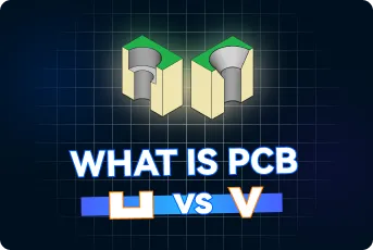
Countersink or Counterbore? Choose Wrong, it Fails.
Countersinks and counterbores are important PCB mechanical features that ensure proper fastener installation, structural integrity, and reliable assembly. This video explains the key differences between these hole types, including when to use a countersink for flush-mounted flat-head screws and when to use a counterbore for recessed socket or hex-head fasteners. It also covers critical design considerations such as screw head compatibility, remaining material thickness, manufacturing tolerances, and plating effects. By selecting and specifying these features correctly, engineers can improve assembly quality, prevent mechanical failures, and enhance the durability of rigid, aerospace, medical, and automotive PCB applications.
-
 00:55
00:55
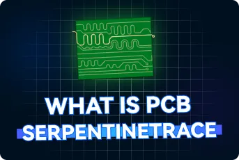
PCB Serpentine Trace: Useful or Risky?
Serpentine traces, also known as meander routing, are widely used in high-speed PCB designs to match signal lengths and ensure synchronized signal arrival. This video explains how serpentine routing helps manage timing skew in parallel buses, memory interfaces, and differential pairs, while also addressing the signal integrity challenges that can arise from improper implementation. It covers key design considerations such as trace spacing, bend geometry, impedance control, reference plane continuity, and differential pair symmetry. By following best practices and applying serpentine routing strategically, engineers can achieve better timing performance, reduce crosstalk, and improve the reliability of high-speed, HDI, and multilayer PCB designs.
- Products & Service
- Company
- About AIVON
- Contact
- News
- Blog
- Certification
-


- Payment
-


2026 AIVON.COM All Rights Reserved