










For a high-volume 2-layer FR4 production run of 5400 pieces (75 sets, 305.65 × 266.4 mm, 1.6mm thickness, 1oz copper, black solder mask), the DFM review of the working files revealed several manufacturability concerns. With a 12x6 panelization using routing and V-CUT elements, plus 100% flying probe testing, even small design details carried significant risks to yield and panel integrity during processing.
Stamp Hole Spacing Risks in Large Panel Layout
From the 2-layer FR4 PCB ( #FR4-20260108-002 ) DFM perspective, the stamp hole (mouse bite) spacing in the panelization design was notably tight. During CAM review, our engineer observed that the spacing between stamp holes on this large panel could compromise structural integrity, especially under the mechanical stresses of routing and depanelization for 75 sets. The working files showed a configuration that left minimal material between perforations.
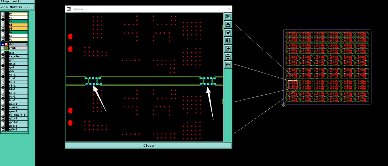
Figure 1: the stamp hole's spacing is too small
Further verification against standard panelization guidelines confirmed the risk. For a board of this size and volume, insufficient spacing increases the chance of premature cracking or chipping during handling and separation. This issue became a key Engineering Question because production could not safely proceed without confirming acceptable spacing to maintain panel stability throughout the fabrication process.
The primary concern was manufacturing stability across the entire 12x6 array. Tight stamp hole patterns can lead to boards detaching unintentionally or sustaining edge damage, directly impacting overall yield in high-volume runs.
Solder Mask Coverage on Bottom Layer Pads
Engineering observation identified two specific bottom-layer pads without designed solder mask openings. With black solder mask specified for the order, the Gerber data showed these pads fully covered by mask. Our team immediately raised an EQ because this configuration risked ink completely covering the pads during application, potentially blocking soldering surfaces.
| Feature | Design Data | Standard Expectation | Risk Level |
|---|---|---|---|
| Stamp Hole Spacing | Tight configuration | Adequate panel strength | High |
| Bottom Pads Solder Mask | No opening | Defined openings | Medium-High |
| Square Metal Slots | Square shape | Milling-friendly geometry | Medium |
Table 1: Primary DFM Risks Identified. This summary highlights the top concerns from the working file review. Stamp hole spacing posed the greatest threat to panel integrity in this high-volume order.
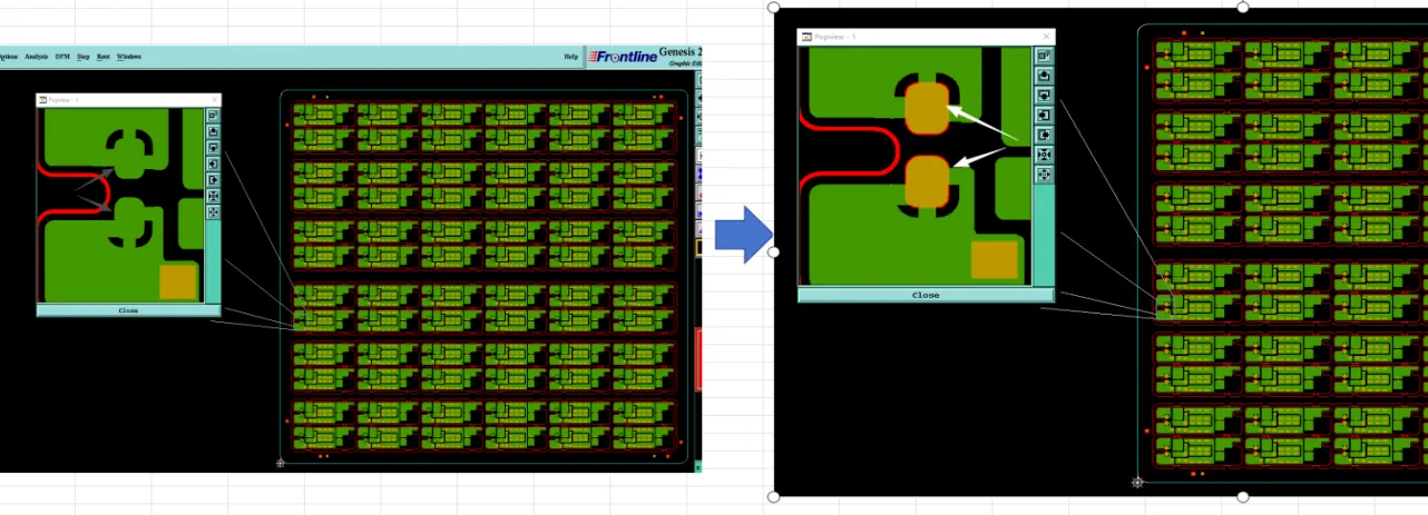
Figure 2: the two pads indicated by the arrow on the bottom layer do not have solder mask openings designed
Verification of the fabrication notes and customer requirements highlighted the mismatch. In black solder mask processes, missing openings often lead to ink bleeding or full coverage on small pads, especially on the bottom side where visual inspection during production is more challenging. This was not a minor cosmetic issue — it directly threatened downstream assembly reliability.
Square Slot Geometry and Tight Tolerance Challenges
The design included square metal slots that are difficult to process cleanly with standard drilling tools. Our CAM engineer noted that sharp corners and square profiles often lead to tool deflection or irregular plating when relying on drilling alone. The specified tolerances for these metal slots were particularly tight relative to typical manufacturing capabilities for this board size and material.
Additional review revealed a silkscreen line that could potentially be misinterpreted as a V-CUT indicator. This ambiguity required confirmation to prevent routing misalignment. Combined with the slot geometry, these details created multiple points where production could deviate from expected outcomes if left unaddressed.
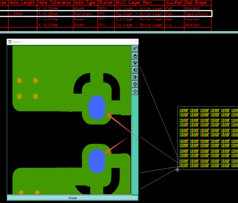
Figure 3: the two slot holes indicated by the arrow are designed bas square slots
Additional review revealed a silkscreen line that could potentially be misinterpreted as a V-CUT indicator. This ambiguity required confirmation to prevent routing misalignment. Combined with the slot geometry, these details created multiple points where production could deviate from expected outcomes if left unaddressed.
In our experience with similar 2-layer panels, such geometry and tolerance combinations frequently trigger EQs because they push the limits of consistent process control across large panel areas.
How Unresolved Issues Threatened Production Yield and Board Reliability
Tight stamp hole spacing, if ignored, could cause panels to break prematurely during routing or mechanical depanelization. This would result in damaged individual boards, increased scrap rates, and production delays for the 5400-piece order. According to common IPC-A-600 considerations, edge quality and panel stability directly influence final board usability.
Ink-covered pads from missing solder mask openings risk poor solderability during assembly, potentially leading to weak joints or open circuits. Square slots with tight tolerances could suffer from incomplete plating or dimensional variation, creating stress points prone to copper peeling or mechanical failure in the field.
Realistic Failure Scenarios Avoided by Engineering Review
Without clarification, the tight stamp holes could have led to boards breaking apart during V-CUT or handling, producing scrap boards and cosmetic edge defects. In high-volume runs, this type of issue has historically caused significant yield loss and rework.
Missing solder mask openings on pads might allow black ink to cover critical areas, resulting in assembly failures such as non-wetting or solder bridging. For the square slots, difficult processing could create irregular edges and plating voids, increasing the likelihood of via-like cracking or delamination under thermal cycling.
Our team prioritized these risks because the consequences in a 75-set production would be amplified across thousands of boards.
Targeted DFM Adjustments for Panel Stability and Process Compatibility
We recommended increasing stamp hole spacing to improve panel strength during depanelization. For the bottom pads, confirmation and addition of proper solder mask openings were advised to ensure clean pad exposure. Square slots were reviewed for possible geometry adjustment or confirmation of milling approach, along with relaxed but manufacturable tolerances.
The silkscreen line was clarified to avoid any confusion with V-CUT paths. These adjustments were discussed with the customer, who provided timely confirmation, allowing the files to move forward with production confidence while maintaining the 13-day lead time.
| Issue | Recommended Action | Expected Benefit |
|---|---|---|
| Stamp Hole Spacing | Increase spacing | Prevent premature panel breakage |
| Solder Mask on Pads | Add openings | Ensure solderability |
| Square Slots | Geometry / tolerance review | Reliable milling and plating |
Table 2: DFM Recommendations Summary. These practical changes directly addressed the highest-risk elements identified in the CAM review for this large panel order.
Strengthening Manufacturing Outcomes Through Early Risk Mitigation
This high-volume case underscores the value of thorough DFM engagement before production. By resolving stamp hole spacing, solder mask coverage, and slot processing concerns early, we minimized the potential for widespread yield loss and ensured the boards would meet both immediate fabrication and long-term reliability needs. Early collaboration on working files continues to be the most effective way to prevent avoidable manufacturing problems.
We encourage designers and sourcing teams to involve DFM review as soon as panelization and critical features are defined, particularly for volume orders where small issues can scale quickly.
FAQ
Q1: Why does stamp hole spacing matter in high-volume panelization?
A1: Insufficient spacing creates weak points that can cause panels to break during routing or handling. This leads to board damage, edge defects, and higher scrap rates, especially problematic in large 12x6 panels.
Q2: What happens if solder mask covers pads without designed openings?
A2: Black solder mask ink can fully cover the pads, preventing proper soldering during assembly. This often results in poor wetting, weak joints, open circuits, or costly rework after delivery.
Q3: Why are square slots challenging for PCB manufacturing?
A3: Square geometries are difficult to produce cleanly with drilling tools and may require milling adjustments. Tight tolerances on such features can lead to irregular plating or dimensional variations that affect mechanical reliability.
Q4: How can early DFM review improve yield in large FR4 orders?
A4: It catches issues like stamp hole weakness, mask coverage problems, and process-incompatible features before fabrication. Addressing them prevents amplified scrap and ensures consistent quality across thousands of boards.
Q5: Should designers always clarify silkscreen lines near V-CUT areas?
A5: Yes. Ambiguous lines can be mistaken for V-CUT paths, leading to incorrect routing or alignment errors. Clear confirmation avoids edge damage and maintains panel integrity.






