










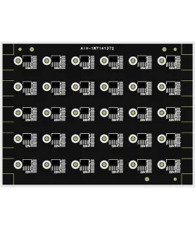
PCB Specifications
| Parameter | Value | Parameter | Value |
|---|---|---|---|
| PCB Type | FR4 PCB | Quantity | 75 pcs |
| Layers | 2 Layers | Board Type | Panel PCB |
| Dimensions | 305.65 x 266.4 mm | Copper Weight | 1oz |
| Thickness | 1.6 mm | Min Track / Spacing | 6/6mil↑ |
| Surface Finish | HASL Lead Free | Min Hole Size | 0.3mm↑ |
| Solder Mask | Black | Silkscreen | White |
| Stack-up | Custom | Impedance Control | No |
Manufacturing Timeline
Logistics Information
Key Manufacturing Processes
Manufacturing Summary
This 2-layer FR-4 board measured 305.65 × 266.4 mm at 1.6 mm finished thickness with 1 oz copper on both sides. The order involved 5400 pieces panelized 12×6, using TG150 material, black solder mask, and lead-free HASL surface finish. Minimum line width of 6 mil fell within conventional geometry, with all vias specified for tenting and mechanical routing for outer contours and slots. Production confirmation was obtained after addressing several DFM points raised during CAM review.
Key issues included missing solder mask openings on two bottom-layer pads, which risked ink coverage and potential hole blocking during application; these were confirmed and adjusted to ensure clean pad exposure. Square slot holes presented tooling challenges for standard drilling, leading to confirmation of rout processing instead. Stamp hole spacing was reviewed as too tight and prone to premature board separation, while metal slot tolerances were verified against achievable process capability. A suspected V-CUT indicator line in the silkscreen layer was clarified to avoid unintended scoring.
All clarifications were resolved prior to production release, allowing full panel utilization and 100% flying probe testing to complete within the 13-day lead time. The boards delivered with consistent quality and no reported separation or tolerance deviations. Details on the stamp hole spacing and slot routing adjustments are covered in the associated engineering case study.
Explore More PCB Manufacturing Resources
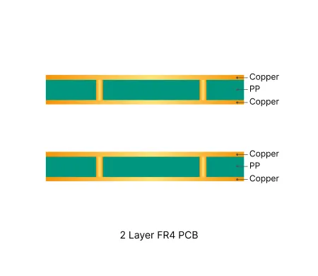
2 Layer FR4 PCB Manufacturing Insights
2 layer FR4 PCBs deliver cost-effective solutions for most electronic designs. Their simple structure enables consistent quality and efficient production cycles.
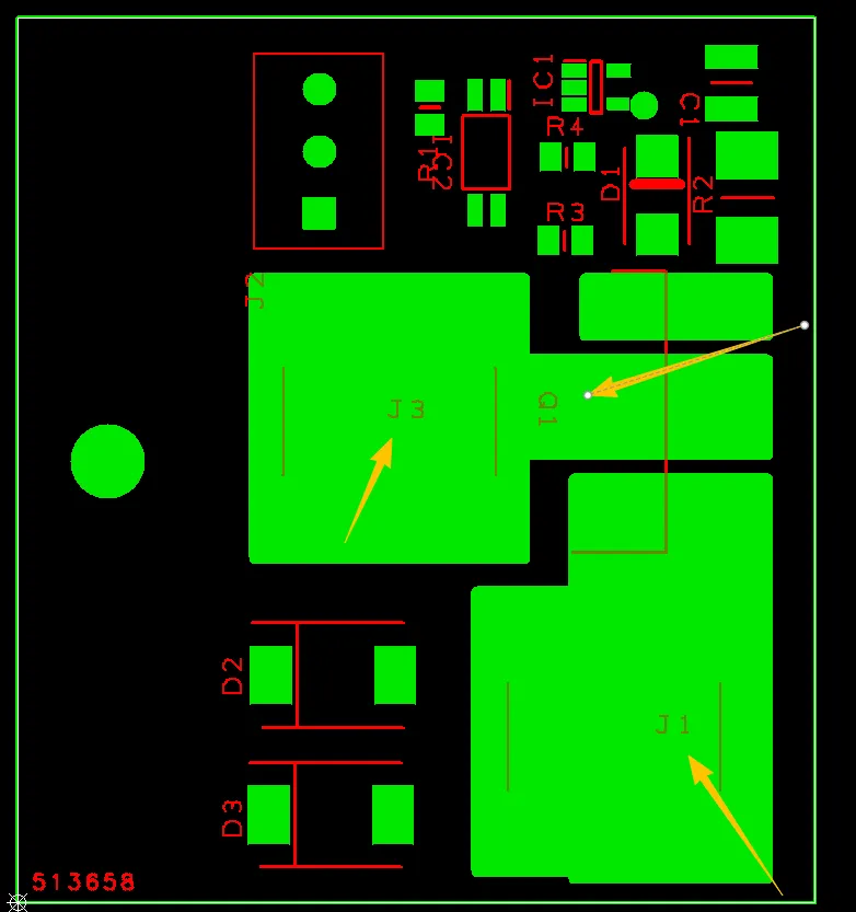
Common Engineering Queries in 2 Layer FR4 PCB Design and Manufacturing
Real Engineering Queries (EQ) and DFM issues for 2 Layer FR4 PCB (double-sided boards) from actual production reviews. Learn how to avoid common problems with via treatment, silkscreen on pads, solder mask openings, hole attributes, board edge clearance, and other frequent design pitfalls.
Real Production Records
| Order ID | PCB Type | Layers | Dimensions | Solder Mask | Surface Finish | Quantity | Action |
|---|---|---|---|---|---|---|---|
| FR4-20260928-023 | FR4 PCB | 1 | 90.5 x 117.5 | Green | HASL Lead Free | 100 | View detail |
| FR4-20260924-035 | FR4 PCB | 2 | 42.67 x 26.55 | Green | HASL Lead Free | 5 | View detail |
| FR4-20260923-016 | FR4 PCB | 2 | 100 x 87 | Blue | HASL Lead Free | 5 | View detail |


