Large 4-layer FR-4 boards with tight hole-to-hole spacing and fine silkscreen markings frequently require detailed DFM adjustments during CAM review. This case examines a 299.5 × 208 mm panelized board using TG130 material. During engineering analysis, several manufacturability issues involving hole compensation, non-plated features, and character sizing were identified, necessitating customer confirmation.
As a senior CAM engineer, I have seen many cases where small design details create significant production risks on standard multilayer boards. In this order, the combination of tight hole spacing and undersized characters triggered targeted Engineering Questions (EQs) to ensure reliable drilling, plating, and legibility.
Order Overview
This was a 4-layer FR-4 board ( #FR4-20260312-048 ) with TG130 material, 1.6mm finished thickness, and 1oz copper on inner and outer layers. The design specified ENIG surface finish, 0.2mm minimum hole size, green solder mask, white silkscreen, and 6mil line width/spacing. Production involved 100% flying probe testing, customer panelization (2x3), V-scoring combined with routing, and mechanical forming. Quantity was 30 pieces.
The large panel size and mix of plated and non-plated holes, along with silkscreen requirements, made precise CAM verification essential to avoid defects in drilling and printing.
Main Engineering Questions Found During CAM Review
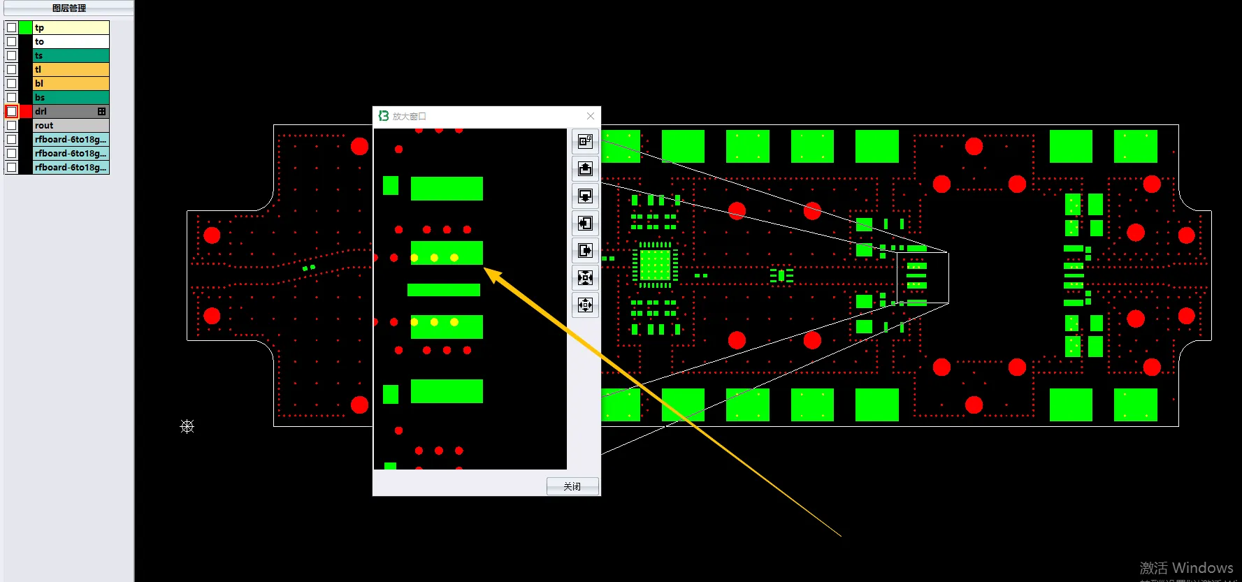
1. Tight Hole-to-Hole Spacing and Compensation Strategy
Multiple locations showed hole-to-hole spacing that was too tight for standard processing. Our CAM team identified that without compensation, the minimum spacing would risk drill breakout or copper residue between holes.
Figure 1: hole-to-hole spacing that was too tight
We noticed this during drill file analysis. Our engineer suggested reducing the affected hole diameters by 0.05mm to maintain safe spacing while preserving functionality. This adjustment was critical for reliable plating and to prevent shorting or weak interconnects in the final board.
If ignored, the tight spacing could have caused hole breakout, incomplete plating, or copper bridging, resulting in open circuits or low yield. On a 1.6mm board with 1oz copper, such issues often lead to scrap after electrical testing.
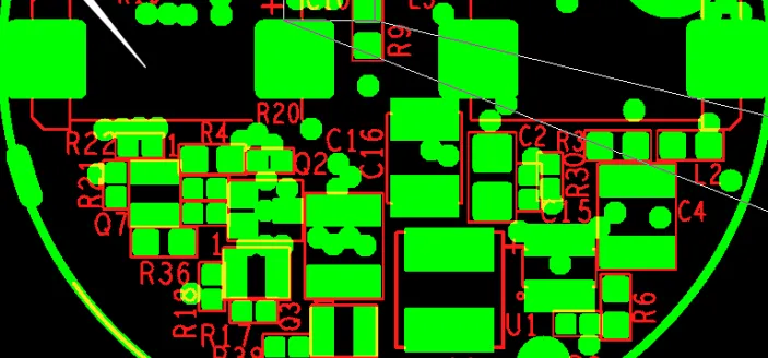
2. Via in Single-Sided Pads on DBR1 Layer Treated as Non-Plated Holes
Certain vias were designed in single-sided pad and located on the DBR1 layer. During our standard CAM review process, we processed these features as non-plated holes (NPTH) according to common manufacturing practice for single-sided pads without through-hole plating requirements.
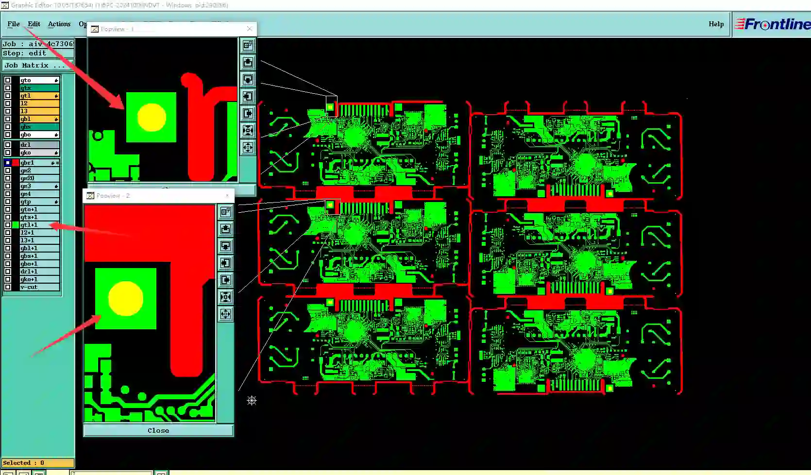
Figure 2: vias were designed in single-sided pad
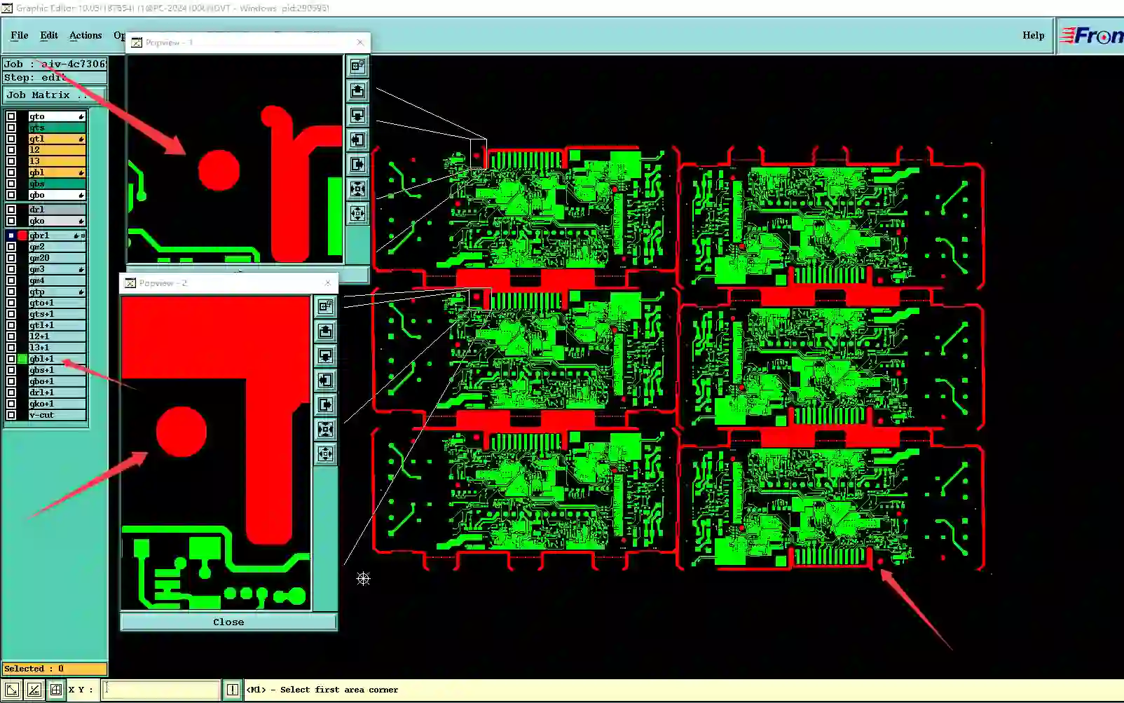
Figure 3: vias located on the DBR1 layer
We noticed this during detailed drill and layer cross-check. Our CAM engineer raised an EQ to confirm that treating them as non-plated holes aligned with the customer's design intent, as plating these features unnecessarily could affect cost, solderability, or mechanical fit in the final assembly.
This clarification is important because single-sided pads on specific layers can be easily misinterpreted. If we had plated them as through holes without confirmation, it could lead to unwanted copper in vias, increased plating time, or interference with component assembly. Conversely, if the customer intended plated holes, treating them as non-plated would result in open circuits or poor connectivity.
In our experience with similar designs, failing to confirm such details often leads to functional failures after assembly or costly rework. After customer confirmation, we proceeded with non-plated processing for these specific holes, ensuring the production data accurately reflected the intended structure. This step helped avoid unnecessary manufacturing variations on this 4-layer board.
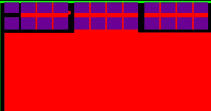
3. Silkscreen Character Height Below Factory Minimum
The design included characters with height below our minimum standard of 0.72mm, particularly on or near pads. We raised an EQ noting that such small text would likely result in incomplete or blurry printing, even if the customer accepted some defect.
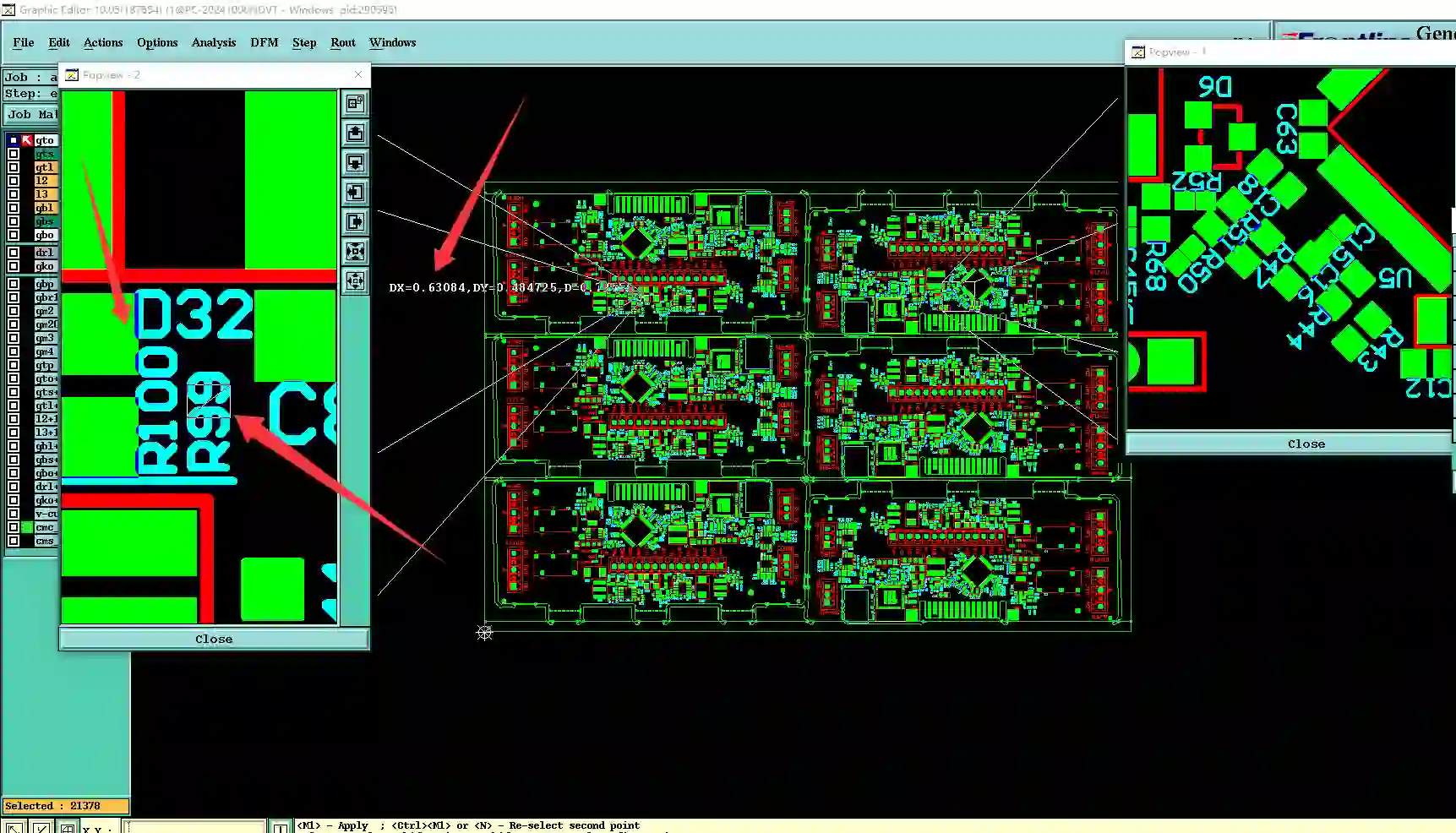
Figure 4: characters with height below our minimum standard of 0.72mm
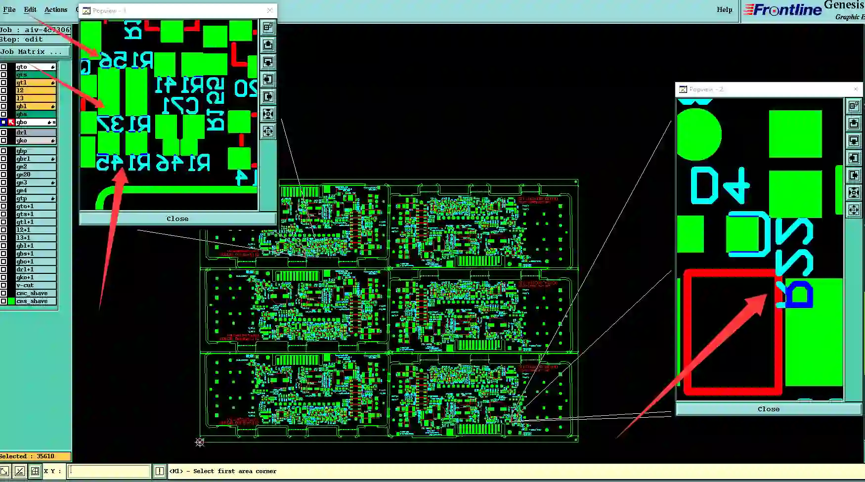
Figure 5: silkscreen character on or near pads
We noticed the issue while reviewing the silkscreen layer. Our CAM engineer recommended increasing character size where possible to ensure legibility for traceability and quality inspection. The customer was informed that we would proceed with the provided data while accepting potential fuzziness.
If not addressed, unreadable markings could lead to traceability problems, assembly errors, or customer rejection during incoming inspection. Small characters on pads also risk solder mask interference or poor cosmetic appearance.
Suggested EQ Categories
Hole & Tolerance Issues
- Tight hole spacing requiring diameter reduction
- Single-sided pad processing on specific layers
Solder Mask & Silkscreen Issues
- Character height below minimum standard
Manufacturing Risks and DFM Insights
Tight hole spacing is a common trigger on multilayer boards. Without adjustment, it leads to drilling defects and yield loss. Similarly, undersized silkscreen characters often cause legibility issues that only appear after printing.
Ignoring the hole spacing EQ could result in breakout or shorts. Small characters risk unreadable markings and quality failures. These issues typically cause delays and extra engineering cycles if not resolved early.
How the Engineering Team Resolved the Issues
Our team provided annotated images showing the tight spacing areas and proposed the 0.05mm hole reduction. For characters, we confirmed acceptance of potential fuzziness while suggesting enlargement where feasible. Single-sided pad handling was verified with the customer.
We noticed the character issue early and adjusted the silkscreen data after confirmation. This ensured production could proceed with minimized risks.
Final Manufacturing Outcome
All EQs were clarified with customer approval. Hole diameters were optimized, markings confirmed, and production files finalized. The order was released for fabrication with updated parameters.
Key Takeaways for PCB Designers
- Maintain adequate hole-to-hole spacing to allow for standard drill compensation without size reduction.
- Design silkscreen characters at or above factory minimum height (0.72mm recommended) for reliable printing.
- Clearly specify treatment for single-sided or non-plated pads in fabrication notes.
- Provide consistent Gerber and supporting files to reduce confirmation cycles.
- Account for silkscreen placement relative to pads to avoid interference.
- Review drill files for tight features before submission.
- Be prepared for DFM suggestions on spacing and marking adjustments.
- Confirm all special processing (plated vs non-plated) early in the review process.
FAQ
Q1: Why reduce hole size for tight spacing?
A1: To maintain safe clearance between holes and prevent breakout or copper residues during drilling and etching.
Q2: What problems occur with undersized silkscreen characters?
A2: Blurry, incomplete, or unreadable markings that affect traceability, assembly, and quality inspection.
Q3: How are single-sided pads typically handled?
A3: Often treated as non-plated holes unless otherwise specified, to avoid unnecessary plating costs and complexity.
Q4: Why is hole spacing critical in multilayer PCBs?
A4: Insufficient spacing risks drill misalignment, breakout, or short circuits, significantly reducing yield.