










In a recent 2-layer FR4 production run for 30 pieces, our DFM review uncovered several manufacturability concerns in the working files that could have impacted yield and long-term reliability. The board featured standard 1oz copper on both sides, 1.6mm thickness, and green solder mask with white silkscreen. While the design appeared straightforward, the combination of via treatments, plated slot processing, and dimensional details required careful engineering clarification before fabrication could proceed safely.
Why This Design Required a Thorough DFM Review
From a DFM perspective, even simple 2-layer boards ( #FR4-20260103-008 ) can harbor hidden risks when working files contain compensated data or ambiguous process requirements. This project specified V-CUT plus routing panelization (2x3 array), lead-free HASL surface finish, and 100% flying probe testing. The customer note explicitly stated these were working files with instructions not to apply additional drill compensation and to pay special attention to plated slots while adding a data code.
Our CAM engineering team immediately identified potential mismatches between the provided data and standard manufacturing processes. The primary concerns centered on via solder mask treatment and plated slot fabrication methods. These issues, if left unaddressed, could compromise both production yield and the board's long-term performance in its intended electronic application.
Via Tenting Mismatch and Plated Slot Processing Conflicts Detected
The engineering review highlighted three key areas requiring clarification, with via solder mask configuration emerging as the highest priority risk.
Via Solder Mask Treatment Inconsistency
Multiple vias in the design showed double-sided open windows in the solder mask layers. However, the process requirements specified tented vias (cover oil). This mismatch created a high risk of ink intrusion into the holes during solder mask application, potential copper exposure at hole mouths after processing, and entrapment of solder beads during assembly.
| Aspect | Provided Data | Process Requirement | Risk Level |
|---|---|---|---|
| Via Solder Mask | Double-sided open windows | Tented (cover oil) | High |
| Plated Slots | Drill-defined | Milling/Routing | Medium |
| Board Dimensions | 317.65 x 175 mm (actual) | 317.69 x 175.01 mm (spec) | Medium |
Table 1: Key DFM Risk Summary. This table captures the primary mismatches identified during CAM review. The via treatment inconsistency posed the greatest threat to both yield and post-assembly reliability.
Plated Slot Processing Method
The customer provided drill data for plated slots, but our standard process for such features uses milling (routing) to ensure clean edges and proper plating quality. Using drilling alone could result in irregular slot walls and plating inconsistencies.
Yield and Reliability Impacts from Unresolved Via and Slot Issues
From a reliability standpoint, vias with unintended open windows increase the likelihood of solder mask ink entering the holes. During HASL, this can lead to incomplete coverage or trapped residues. According to IPC-A-600 acceptability criteria, exposed copper at via mouths or inconsistent solder mask coverage can accelerate oxidation and compromise long-term electrical integrity.
For plated slots, improper processing methods risk dimensional inaccuracies and poor edge quality, potentially causing assembly alignment issues or mechanical stress concentrations. The minor dimensional discrepancy, while small, could affect panelization fit and fiducial recognition during automated processes if not aligned with fabrication tolerances.
| Risk Factor | Potential Yield Impact | Reliability Concern |
|---|---|---|
| Open Via Windows | Ink blockage, reduced test probe contact | Solder bead entrapment, corrosion |
| Slot Processing | Edge roughness, plating voids | Mechanical weakness, assembly misalignment |
Table 2: Risk Impact Assessment. Comparing yield and reliability implications helps prioritize preventive actions during DFM review. Via issues carried the highest combined risk profile for this 2-layer board.
Manufacturing Failure Modes Prevented in This FR4 Production Run
If the double-sided open vias had proceeded without clarification, several realistic manufacturing failures could have occurred. During solder mask application, ink could flow into the vias, leading to partial or complete blockage. In the HASL process, this would trap solder beads inside the holes, creating hidden defects that might pass electrical testing initially but cause intermittent connections or shorts during thermal cycling in the field.
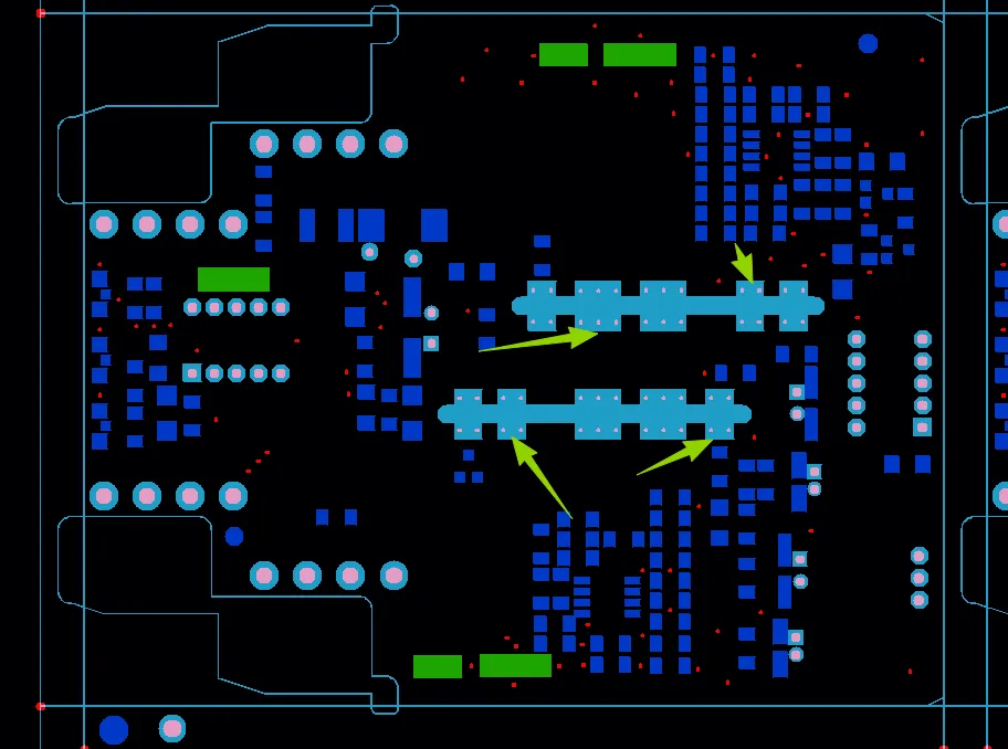
Figure 1: some vias are designed with openings on both sides
Exposed copper at via entrances after processing could oxidize rapidly, leading to poor solderability during customer assembly. In extreme cases, this has resulted in open circuits or high-resistance paths that only manifest after deployment, causing costly field failures and warranty claims.
For the plated slots, drilling instead of milling could produce rough walls with plating nodules or thinning, increasing the risk of copper peeling under mechanical stress or thermal expansion. The dimensional tolerance difference, though minor, could lead to panelization misalignment, affecting V-CUT quality and causing edge chipping or board separation issues during depanelization.
Our team has seen similar cases where ignored via tenting requirements led to scrap rates exceeding 20% due to post-assembly defects. Preventing these outcomes through early EQ communication protects both production efficiency and product reliability.
Specific DFM Recommendations for Via Tenting and Slot Fabrication
We issued targeted Engineering Questions (EQs) to resolve each concern. For the vias, we recommended switching to full solder mask tenting or, alternatively, confirming acceptance of green oil plugging for better hole protection. This change aligns the design with the stated process requirements and significantly reduces ink intrusion and solder entrapment risks.
Regarding plated slots, we confirmed the need to use milling rather than relying solely on drill data, ensuring cleaner slot profiles and consistent plating thickness. For dimensions, we verified the exact outline to use (317.69 x 175.01 mm) and adjusted panelization accordingly. Tolerance confirmations for holes and traces were established based on working file compensation: via holes at -0.05 ±0.05mm, PTH at -0.15 ±0.075mm, and trace width at ±20%.
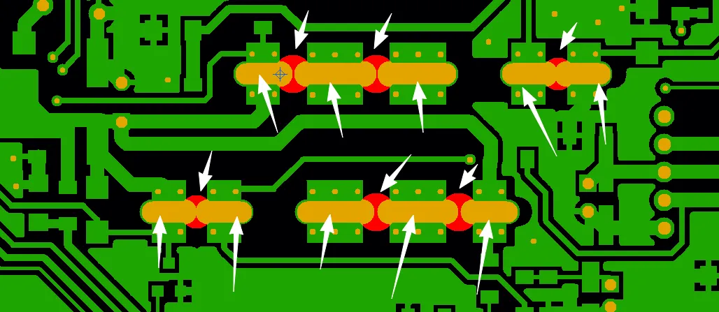
Figure 2: we propose modifying the process to milling
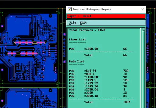
Figure 3: drilling diameter tolerance and line width tolerance control
The customer collaborated effectively, providing clarifications that allowed us to proceed with production-ready files. These adjustments ensured compatibility with our 55mm routing length capability, 0.3mm minimum hole size, and overall panel utilization.
| Issue | Recommendation | Benefit |
|---|---|---|
| Via Open Windows | Implement tenting or green oil plug | Eliminates ink/solder risks |
| Plated Slots | Use milling process | Improved edge quality and plating |
| Dimensions | Align to spec 317.69×175.01mm | Ensures panelization accuracy |
Table 3: DFM Recommendations and Outcomes. Proactive adjustments like these directly translate to higher first-pass yield and more reliable finished boards.
Achieving Reliable Production Through Proactive Via and Dimension Clarification
This case demonstrates how early DFM intervention prevents small discrepancies from becoming major production issues. By addressing via treatment, slot processing, and tolerances before lamination and drilling, we protected the 30-piece order from potential scrap and ensured the boards met both electrical testing and long-term reliability expectations.
Engaging in thorough engineering review before production starts remains one of the most effective ways to minimize risks in PCB fabrication. We encourage designers to share working files early and collaborate closely on process confirmations. This approach not only improves yield but also builds confidence in the final product's performance.
FAQ
Q1: Why can double-sided open vias create problems even in a simple 2-layer design?
A1: Open windows allow solder mask ink to enter the holes during application, potentially blocking them or leaving residues. Combined with HASL, this increases the risk of trapped solder beads and exposed copper, which can lead to corrosion or poor contact reliability over time.
Q2: What happens if plated slots are processed using drill data instead of milling?
A2: Drilling alone often results in rougher edges and inconsistent plating thickness. Milling provides cleaner, more precise slots that better withstand mechanical stress and ensure uniform copper deposition, reducing assembly and reliability risks.
Q3: How does a small dimensional discrepancy affect PCB manufacturing?
A3: Even minor differences (e.g., 0.04mm) can impact panelization, V-CUT alignment, and fiducial recognition. This may cause edge defects, depanelization issues, or problems in automated assembly equipment.
Q4: Why is confirming tolerances important for working files?
A4: Working files often include pre-compensation. Without confirming exact tolerances for holes and traces, the final board may deviate from design intent, affecting impedance (if critical), solder mask registration, or electrical performance.
Q5: How does proactive DFM review improve overall PCB yield?
A5: By identifying and resolving mismatches in via treatment, slot processing, and dimensions early, DFM prevents defects that would otherwise appear during fabrication, testing, or assembly, often reducing scrap and rework significantly.
Q6: When should designers engage DFM support for 2-layer boards?
A6: As soon as working files are ready, especially when using compensated data or non-standard features like plated slots. Early review allows time for adjustments without delaying the overall project timeline.






