










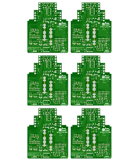
PCB Specifications
| Parameter | Value | Parameter | Value |
|---|---|---|---|
| PCB Type | FR4 PCB | Quantity | 5 pcs |
| Layers | 2 Layers | Board Type | Panel PCB |
| Dimensions | 175.01 x 317.69 mm | Copper Weight | 1oz |
| Thickness | 1.6 mm | Min Track / Spacing | 3/3mil |
| Surface Finish | HASL Lead Free | Min Hole Size | 0.3mm↑ |
| Solder Mask | Green | Silkscreen | White |
| Stack-up | Custom | Impedance Control | No |
Manufacturing Timeline
Logistics Information
Key Manufacturing Processes
Manufacturing Summary
This 6-layer FR-4 board measured 317.65 × 175 mm with 1 oz copper on outer layers and 0.5 oz inner layers. Minimum trace/space of 5/5 mil placed it in tighter geometry territory, paired with controlled impedance and mixed via treatments. Production used standard mechanical drilling for PTH and NPTH, with routing for the specified slot features after confirming process requirements against the supplied working gerber. Overall panel utilization remained efficient for the 100-piece quantity.
Several DFM points required clarification during CAM review. Double-sided open windows on selected vias introduced risks of solder mask ink entering holes and subsequent tin bead entrapment during assembly; these were resolved by confirming cover oil application where process capability allowed, reducing potential assembly defects. Dimension tolerance between supplied data (317.65 × 175 mm) and process target was adjusted with customer approval. Slot and round hole definitions were aligned from drill to rout as needed, while hole diameter and trace width tolerances followed the agreed via -0.05/+0.05 mm and line ±20% specification to maintain reliability. Edge interface height variations noted in the gerber were reviewed to ensure post-routing flatness.
All adjustments were implemented prior to lamination and plating, with final electrical testing confirming impedance and continuity within limits. The order completed on schedule with consistent surface quality. For full details on the via windowing and mask plugging resolution, refer to the related engineering case study.
Explore More PCB Manufacturing Resources
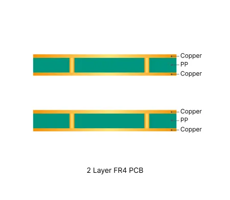
2 Layer FR4 PCB Manufacturing Insights
2 layer FR4 PCBs deliver cost-effective solutions for most electronic designs. Their simple structure enables consistent quality and efficient production cycles.
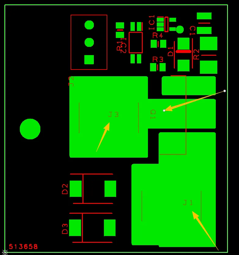
Common Engineering Queries in 2 Layer FR4 PCB Design and Manufacturing
Real Engineering Queries (EQ) and DFM issues for 2 Layer FR4 PCB (double-sided boards) from actual production reviews. Learn how to avoid common problems with via treatment, silkscreen on pads, solder mask openings, hole attributes, board edge clearance, and other frequent design pitfalls.
Real Production Records
| Order ID | PCB Type | Layers | Dimensions | Solder Mask | Surface Finish | Quantity | Action |
|---|---|---|---|---|---|---|---|
| FR4-20260928-023 | FR4 PCB | 1 | 90.5 x 117.5 | Green | HASL Lead Free | 100 | View detail |
| FR4-20260924-035 | FR4 PCB | 2 | 42.67 x 26.55 | Green | HASL Lead Free | 5 | View detail |
| FR4-20260923-016 | FR4 PCB | 2 | 100 x 87 | Blue | HASL Lead Free | 5 | View detail |


