Introduction
Rigid-flex PCBs continue to challenge even experienced designers due to the inherent differences in material behavior, thickness tolerances, and processing requirements between the rigid FR-4 sections and flexible polyimide areas. In this real production order, a 6-layer hybrid design with a 1x4 panelization and tight 6 mil line/space features required multiple engineering questions (EQs) during our CAM review process.
Our CAM team identified several manufacturability concerns around the rigid-flex transition zone, stackup tolerances, inner layer copper patterns, and feature details that could impact yield. These issues are typical for rigid-flex boards where design intent often meets factory process limitations. Raising EQs before production is our standard practice to prevent scrap, ensure mechanical reliability at the flex-rigid junction, and maintain electrical performance.
This case study walks through the actual engineering review, the risks we mitigated, and practical DFM lessons for designers working on similar hybrid constructions.
Order Overview
This was a 6-layer rigid-flex PCB ( #RFP-20260127-036 ) with overall dimensions of 149.1 × 209.3 mm. The rigid portion uses Shengyi FR-4 (S1150G) material with a TG of 155°C, while the flexible section is 2-layer using Shengyi SF305C polyimide at 0.18 mm nominal thickness. Total board thickness was specified at 1.2 mm for the rigid area.
Key parameters included 1 oz copper on inner and outer layers, ENIG surface finish with 1.00 μm minimum gold thickness, minimum hole size of 0.2 mm, and 6 mil minimum line width/space. The order called for 100 pcs (25 sets) with 1x4 panelization using V-scoring and router separation. Flying probe full electrical testing was required, along with electrical performance reports and quality certificates. Special processes included point glue at the rigid-flex junction and reference to a previous version for stackup and fabrication notes.
The combination of hybrid materials, controlled impedance expectations (though not formally documented), and precise mechanical features at the transition zone made this a classic case requiring careful CAM engineering validation before releasing to production.
Main Engineering Questions Found During CAM Review
Stackup Confirmation and Thickness Tolerances at Rigid-Flex Junction
One of the first critical issues we identified was the need to confirm the exact stackup and thickness tolerances. After reviewing the Gerber files against the previous version, our engineer suggested confirming: rigid board thickness 1.2 mm ±0.12 mm, flexible area 0.17 mm ±0.05 mm, and total FR4+FPC thickness around 0.7 mm ±0.1 mm, with 1 oz copper inner and outer.
Figure 1: rigid-flex PCB stackup
We noticed the hybrid transition zone is particularly sensitive to thickness variation. Flexible materials exhibit different Z-axis expansion compared to FR-4, which can lead to stress concentrations during lamination and subsequent assembly. If these tolerances were ignored, the board could suffer from delamination at the junction or excessive warpage, especially with the specified 0.5 mm top reinforcement and point glue requirements.
Our CAM team referenced prior production data and proposed the stackup using Shengyi materials on both rigid and flex sections for consistency. The customer confirmed, allowing us to lock the parameters and reduce risk of mechanical failure during bending or thermal cycling.
Point Glue Application at Rigid-Flex Intersection
The order notes specifically required double-sided transparent point glue at the rigid-flex transition (marked with red arrows in the reference drawing), with width controlled at 1.5 ±0.5 mm. This is a common reinforcement method, but precise placement and width control are essential.

Figure 2: double-sided transparent point glue at the rigid-flex transition
Our engineer confirmed the location and dimensions with the customer. Without clear agreement, misalignment could cause adhesive overflow onto functional areas or insufficient coverage, leading to flex cracking or delamination under repeated bending. If ignored, the junction might experience copper peeling or open circuits after thermal stress in assembly.
Inner Layer Mesh Pattern Optimization
We noticed the inner layer grid pattern in the flexible area differed from our standard manufacturing approach. Our suggestion was to change it to our conventional copper skin plus flow glue slot pattern to ensure better resin flow and bonding during lamination.
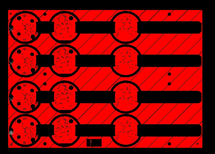
Figure 3: inner layer grid pattern in the flexible area
The customer accepted the change referencing the previous version. This adjustment helps prevent resin voids and improves overall flatness. If the original isolated grid had been used without optimization, it could have resulted in incomplete filling, leading to weak bonding and potential layer separation under mechanical stress.
Silkscreen Optimization and Marking Requirements
Silkscreen adjustments were needed for several pads where characters overlapped. Our team optimized by moving characters where possible and covering others as shown in the review markup (blue areas covered, purple+red for final production). We also added the production cycle code and UL94V-0 marking in the soft board area per customer requirements.
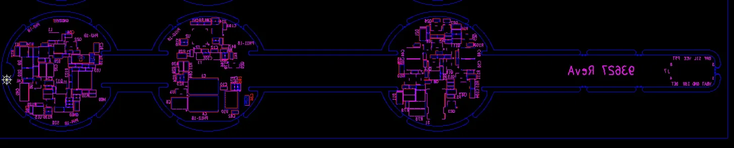
Figure 4: silkscreen optimization
These changes ensure legibility and compliance without affecting solderability. Minor as it seems, poor silkscreen registration near small pads can cause cosmetic defects or assembly confusion.
Mechanical Feature Adjustments: Corners, Stamp Holes, and Pad Sizes
During the CAM review, several mechanical features required clarification and optimization to improve manufacturability and long-term reliability.
Our engineer noticed that the four corners of the panel had sharp right angles, which are prone to scratching and chipping during handling, depanelization, and shipping. We recommended changing them to R1 rounded corners. If left unaddressed, these sharp corners could lead to cosmetic defects, edge damage, or even minor delamination under mechanical stress.
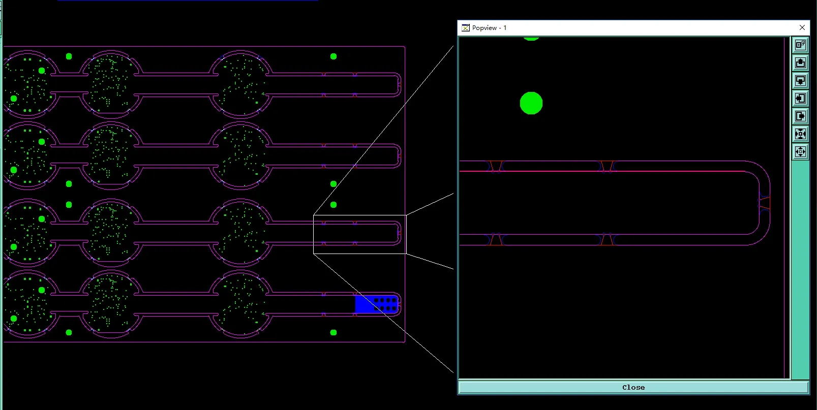
Figure 5: changing the sharp right angles to R1 rounded corners
In the flexible bending area, the original design included stamp holes at the connection positions. We suggested removing these stamp holes entirely and modifying the bending corners to an inverted octagon shape, consistent with our previous successful production version. Stamp holes in flex zones often become stress concentration points, increasing the risk of tearing or cracking during repeated flexing. Ignoring this could result in open circuits or mechanical failure after assembly.
Additionally, the bottom layer had four small pads sized at only 0.25 mm. Due to the limited annular ring on such small features, especially on flexible material, our CAM team recommended increasing the pad diameter to 0.3 mm and applying an inner solder mask opening of 0.26 mm. This adjustment provides better plating reliability and reduces the chance of pad breakout or poor solderability. If the original 0.25 mm pads had been produced as-is, it could have caused low yield, via/pad lifting during SMT, or unreliable electrical connections in the final product.
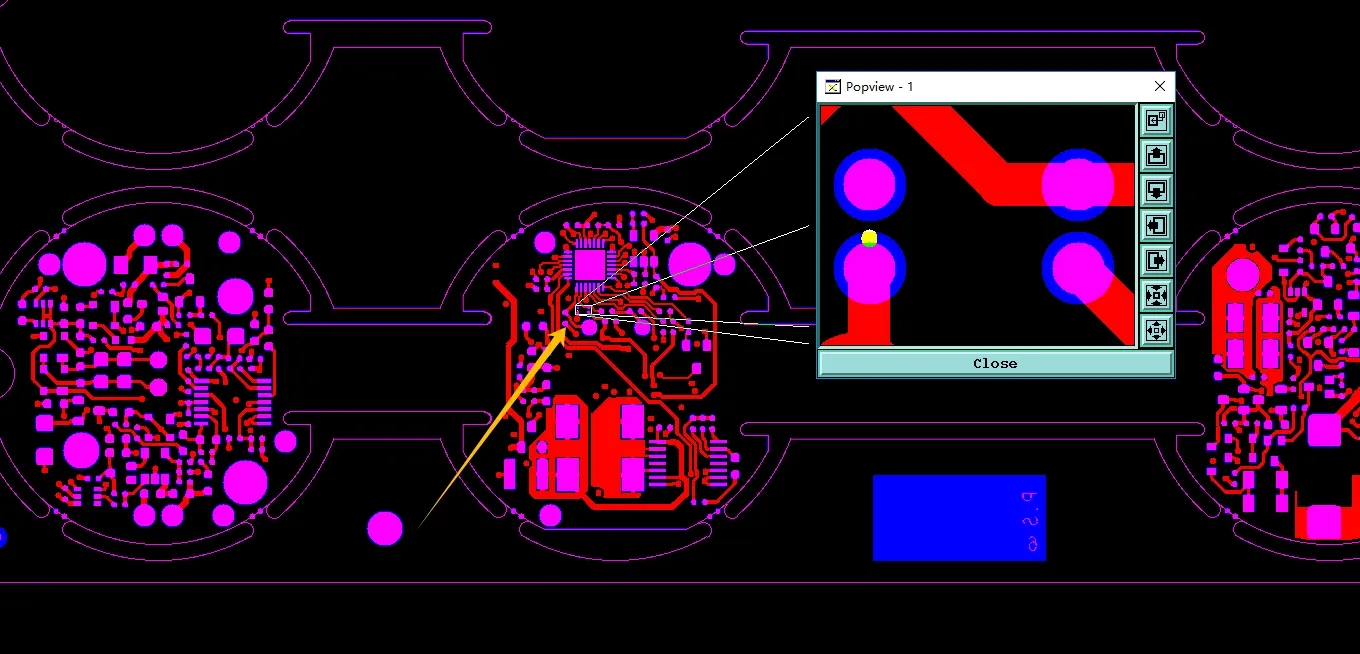
Figure 6: four small pads sized at only 0.25 mm
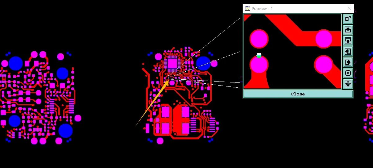
Figure 7: increasing the pad diameter to 0.3 mm and applying an inner solder mask opening of 0.26 mm
The customer confirmed all these mechanical optimizations referencing the previous A version production files. These changes were implemented in the final working gerbers to ensure robust mechanical performance and higher production yield.
Manufacturing Risks and DFM Insights
This case highlighted several common pitfalls in rigid-flex design. Thickness variation across hybrid sections is one of the top triggers for EQs. Without confirmation, warpage or delamination risks increase significantly. The junction point glue and inner layer pattern changes directly impact mechanical reliability — issues that are difficult to fix post-fabrication.
Small pad sizes near minimum tolerances also frequently require adjustment. In this instance, the 0.25 mm pads carried a high risk of breakout or poor plating. Ignoring such details could lead to assembly failures, reduced yield, and costly rework.
How the Engineering Team Resolved the Issues
Our engineering team compiled all EQs with annotated drawings and reference to the previous version. The customer responded promptly, confirming the stackup, glue application, pattern changes, and mechanical optimizations. We updated the working gerbers accordingly, performed a final DFM check, and released the order for production with adjusted panelization features and controlled tolerances.
By addressing these points early, we avoided potential scrap from warpage, junction weakness, or feature-related defects. The 22-day delivery timeline remained on track.
Final Manufacturing Outcome
All engineering clarifications were resolved. The stackup was locked, mechanical features optimized, and production data updated. The order was approved for fabrication with full flying probe testing to verify electrical integrity.
Key Takeaways for PCB Designers
- Always provide clear stackup drawings with tolerance ranges for rigid-flex designs, especially at transition zones.
- Reference previous production versions when applicable to speed up CAM review.
- Consider manufacturability of small pads — increase size where possible and define solder mask openings clearly.
- Avoid sharp corners and stamp holes in flex bending areas; use rounded features and proper relief cuts.
- Coordinate silkscreen placement early to avoid conflicts with pads and ensure required markings fit in designated areas.
- Document special processes like point glue with precise location and dimension callouts.
- Prepare inner layer patterns with factory-standard copper and resin flow considerations in mind.
FAQ
Q1: Why is precise thickness tolerance confirmation critical in rigid-flex PCBs?
A1: Rigid and flex materials have different coefficients of thermal expansion. Unconfirmed tolerances can cause excessive stress at the junction, leading to delamination, warpage, or via cracking during lamination and assembly.
Q2: What risks arise from small pads on flexible circuits?
A2: Pads at 0.25 mm or below are prone to breakout during drilling, poor plating, and lifting during soldering. Increasing to 0.3 mm with appropriate mask openings significantly improves reliability.
Q3: Why do factories recommend changing inner layer mesh patterns in flex areas?
A3: Standard copper skin plus flow glue slots ensure better resin filling and bonding, reducing voids and improving mechanical strength compared to isolated grids.
Q4: Why round corners and modify stamp holes in flex-rigid panels?
A4: Sharp corners are easily scratched during handling. Stamp holes in bending zones can initiate tears. Rounded R1 corners and inverted octagons improve durability and handling safety.
Q5: How does point glue at the rigid-flex junction help?
A5: It provides strain relief and reinforcement. Controlled width (e.g., 1.5 ±0.5 mm) prevents overflow while ensuring the junction withstands repeated flexing without copper peeling or layer separation.
Q6:What is the benefit of early CAM EQ communication?
A6: It prevents production delays, reduces scrap risk, and ensures the final board meets both design intent and manufacturing capabilities, saving time and cost for all parties.