NOR and NAND Flash Application Circuits
Technical guide to flash memory interfaces and reference circuits, covering NAND flash operation, SPI/NOR wiring, debugging practices, and a concise 3D XPoint overview.
Memory & Storage Technology forms a cornerstone of modern electronics, encompassing the hardware and methodologies that enable data retention, retrieval, and management in devices ranging from smartphones to enterprise servers. This category delves into the intricate world of memory types such as DRAM, SRAM, and NAND flash, alongside storage solutions like solid-state drives and hard disk drives. By exploring these elements, readers gain a deeper understanding of how they integrate into printed circuit boards and larger systems, influencing performance, reliability, and efficiency in everyday applications. Professionals and enthusiasts alike will find valuable resources here, including detailed guides on selecting the right memory modules for specific projects, tutorials for implementing storage interfaces like PCIe and SATA, and insights into optimizing data throughput in embedded systems. Best practices for error correction, data security, and thermal management are highlighted, drawing from real-world scenarios in industries such as automotive electronics, cloud computing, and IoT deployments. These articles address common challenges, such as mitigating data corruption in high-vibration environments or scaling storage for big data analytics, providing actionable knowledge that bridges theory and practice. As technology evolves, staying informed on advancements like 3D NAND architecture and emerging non-volatile memory options becomes essential for innovation. The content in this category equips you with the tools to navigate these developments, whether designing compact wearables or robust data centers. Reading through the diverse topics offers a comprehensive view of how memory and storage underpin the digital age, fostering better decision-making and technical proficiency in your work.
Technical guide to flash memory interfaces and reference circuits, covering NAND flash operation, SPI/NOR wiring, debugging practices, and a concise 3D XPoint overview.
Technical overview of DDR4 advancements, highlighting POD termination, bank-group architecture and point-to-point topology compared with DDR3 for higher speed and lower voltage.
Device teardown finds SK Hynix parts: H58GG6MK6GX037 12GB LPDDR5 DRAM and HN8T25DEHKX077 512GB UFS 3.1, both marked CS and likely entering production around 2021.
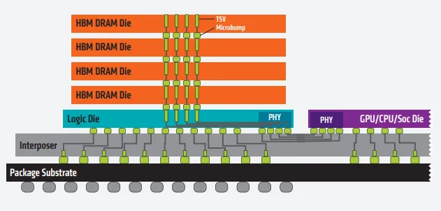
Technical overview of DDR DRAM and HBM standards to guide SoC designers in selecting memory technologies for performance, power, and bandwidth trade-offs.
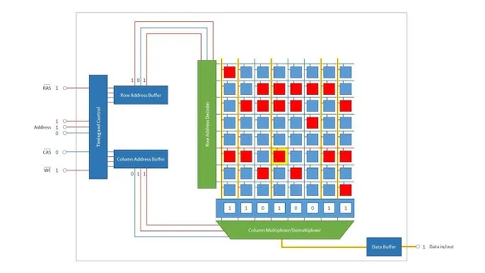
Overview of DRAM types, storage cell structure, and data handling, covering SDRAM/DDR generations, capacitor–transistor cells, and refresh cycles.
Comparison of DDR4 3200 and DDR4 3600 memory: frequency, theoretical bandwidth, performance impact across workloads, and implications of mixing modules for stability.
Analysis of AI storage requirements for large models, detailing Huawei's OceanStor A310 and FusionCube A3000 solutions, scalability, performance, and deployment challenges.
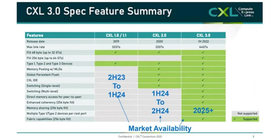
Technical overview of Rambus product portfolio, DDR5 vs DDR4 performance gains, and CXL adoption, covering memory interface chips, IP, security, and acquisitions.
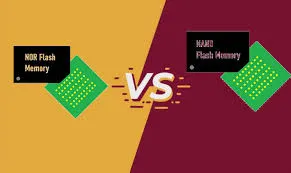
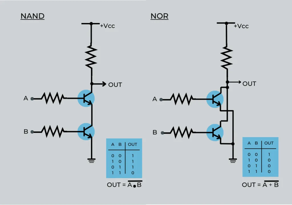
Technical comparison of NAND Flash and NOR Flash memory covering architecture, interfaces, performance, endurance, SPI NAND, applications, and guidance for selecting flash.
Technical overview of OTP and MTP non-volatile memory, comparing eFuse and anti-fuse mechanisms, programmability, security, and application trade-offs.
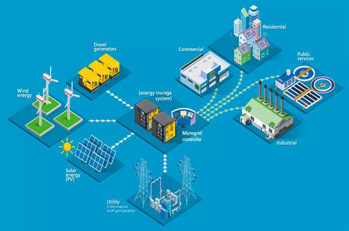
Technical summary of C&I energy storage design: battery selection, BMS/EMS roles, PCS converter functions, modular intelligent architectures, and refined control requirements.
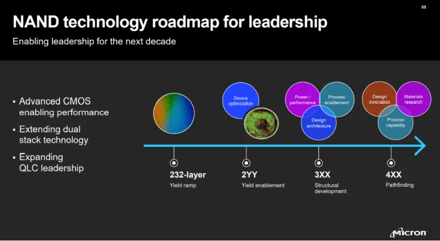
Analysis of 3D NAND development and competing 300+ layer approaches—dual/triple-stack and eight-plane architectures from Samsung, SK Hynix, Kioxia/WD, and performance trade?offs.