Why is Component Lead Forming Critical in Electronics Manufacturing?
Component lead forming is the precise shaping of an electronic component’s wires, or “leads,” to ensure they fit correctly onto a printed circuit board (PCB). This process is vital for through-hole technology, where components like resistors, capacitors, and diodes are inserted into pre-drilled holes and then soldered. Proper lead formation guarantees secure physical mounting, safeguards components from damage, and maintains the electrical integrity of the circuit.
Failing to form leads accurately can lead to intermittent connections, excessive mechanical stress on components, or undesirable short circuits. Leads that are too long might inadvertently contact neighboring traces or components, creating an electrical fault. Overly short leads might not extend sufficiently through the PCB for a strong solder joint. Mastering lead forming is indispensable for both manual and automated assembly workflows, enhancing the longevity and efficiency of the final electronic product. Industry standards such as IPC-A-610 emphasize these requirements to ensure consistent quality across assemblies.
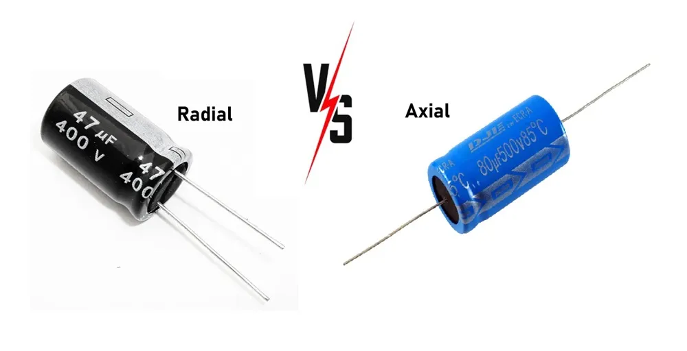
Understanding Different Component Lead Types: Axial vs. Radial
Axial Component Lead Characteristics
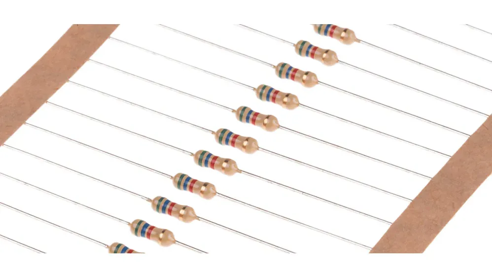
Axial components feature leads extending from opposing ends of their cylindrical or bar-shaped body. Common examples include resistors and certain diodes. Their leads are collinear with the component’s main axis, requiring specific bends to span the distance between widely spaced holes on a PCB. According to IPC J-STD-001, leads must extend at least one lead diameter (or a minimum of 0.8 mm) from the body before any bend to avoid internal damage.
Radial Component Lead Characteristics
Radial components have leads originating from a single side of the component body and running parallel to each other. Electrolytic capacitors commonly use this configuration. These leads typically require minimal bending but demand precise alignment to ensure the component sits correctly without strain. IPC-A-610 criteria stress proper coplanarity and alignment to support reliable solder joints.
Best Practices for Axial Lead Forming
Step-by-Step Axial Lead Preparation
1. Measure Hole Pitch: Begin by accurately measuring the spacing between the mounting holes on your PCB. Standard through-hole designs typically have pitches ranging from 2.54 mm (0.1 inches) to 12.7 mm (0.5 inches).
2. Employ Proper Tooling: Always use specialized lead bending pliers with rounded jaws or dedicated forming jigs. Bending leads by hand can result in inconsistent shapes and potential damage to the component or lead.
3. Ensure Safe Bend Distance: Position the bend at least 1-2 mm away from the component body. This clearance prevents internal damage or cracking, especially for sensitive components. A typical quarter-watt resistor, for example, can safely accommodate a bend radius of approximately 0.8 mm.
Related Reading: Resistor Principles and Manufacturing Types
4. Achieve 90-Degree Angles: For most axial components, bend the leads to a precise 90-degree angle. Symmetrical bends on both leads are crucial for a stable and aesthetically pleasing fit.
5. Trim Excess Length: Once the component is inserted, trim the leads to extend about 1-2 mm beyond the PCB’s surface. This length is ideal for robust soldering without creating excess material that could lead to shorts.
Recommended Lead Forming Parameters (per IPC Standards)
| Parameter | Axial Leads Recommendation | Radial Leads Recommendation | Reference Standard |
|---|---|---|---|
| Minimum distance from body to bend | 0.8 mm or 1× lead diameter | Minimal adjustment only | IPC J-STD-001 |
| Bend angle / alignment | Precise 90° symmetrical bends | Parallel alignment to hole pitch | IPC-A-610 |
| Maximum allowable damage | <10% of lead diameter/width | <10% of lead diameter/width | IPC-A-610 |
| Post-trim protrusion | 1–2 mm (Class 2/3 preferred) | 1–2 mm for flush seating | IPC-A-610 |
| Bend radius (minimum) | 1× lead diameter (e.g., ~0.8 mm for ¼-watt resistor) | N/A (minimal bending) | IPC-7251 / industry practice |
Key Considerations for Axial Lead Forming
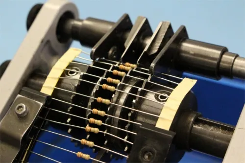
● For consistent results, use component lead forming devices or jigs for mass production.
● Avoid creating sharp creases in the leads, as these can weaken the metal; instead, aim for smooth, gentle radii.
● Handle components delicately to prevent mechanical stress, as components with ceramic or glass bodies are particularly susceptible to cracking from excessive force.
Achieving Precision with Radial Lead Forming
Radial Lead Adjustment Techniques
- Verify lead pitch (often 5 mm or 10 mm) against PCB holes.
- Make gentle adjustments only if needed using precision tools.
- Ensure the component seats flush (typically 2–3 mm above board).
- Insert leads carefully without force.
Best Practices for Radial Lead Handling
● Minimize lead bending for radial components to reduce stress on both the leads and the component body.
● For high volume PCB assembly, utilize a lead forming jig to maintain consistent lead uniformity.
● Always confirm the correct polarity for components such as electrolytic capacitors, as incorrect orientation can result in circuit malfunction.
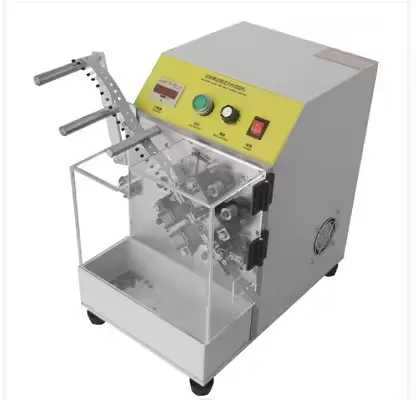
Essential Tools for Accurate Lead Bending
Selecting proper tools enhances quality and efficiency in component lead forming.
- Needle-nose pliers with rounded tips prevent nicking.
- Lead forming jigs provide uniform bends for axial components.
- Automated component lead forming devices process thousands of parts per hour with 0.1 mm accuracy.
- Precision flush cutters trim leads cleanly.
These tools help meet IPC-A-610 acceptability criteria and reduce damage risk.
Related Reading: Beyond Pick and Place: Advanced Robotics in Automated PCB Assembly
Optimal Lead Cutting Techniques for a Professional Finish
After leads are properly formed and components are inserted, trimming excess lead length is the final critical step. Adhering to lead cutting best practices ensures a clean, professional appearance and prevents issues during subsequent soldering or product operation.
Effective Lead Trimming Strategy
● Cut Post-Insertion: Always trim leads after the component is securely seated in the PCB to prevent any misalignment.
● Maintain Adequate Length: Trim leads to a length of 1-2 mm extending beyond the PCB surface. This provides sufficient material for a strong solder joint without creating excess that could cause shorts or interfere with adjacent components.
● Utilize Sharp Cutters: Dull cutting tools can crush or deform leads, which negatively impacts solder joint quality. Employ sharp, precision flush cutters for consistently clean cuts.
● Angle the Cut: Trimming leads at a slight angle (around 45 degrees) can create a pointed tip, which often aids in optimal solder flow during the assembly process.
● Manage Debris: Perform lead cutting over a containment tray or use a tool equipped with a debris catcher. This prevents small metal clippings from scattering across the workspace or PCB, where they could potentially cause short circuits.
Proper lead cutting not only improves the visual appeal of the circuit board but also significantly contributes to its overall reliability. Industry studies on assembly defects indicate that leaving leads excessively long on densely packed boards can elevate the risk of short circuits by as much as 15%.
Addressing Common Challenges in Leaded Assembly
Even with meticulous techniques, leaded assembly can present its own set of challenges. Here are frequent issues and their respective solutions for a smoother process:
● Component Damage: Excessive force during bending is a primary cause of component cracking or breakage. Always use tools specifically designed for lead forming and handle components with care.
● Inconsistent Bends: Manual bending frequently results in uneven lead forms. For uniformity, especially in larger production volumes, rely on jigs or automated forming equipment.
● Lead Stress: Bending leads too close to the component body can weaken the lead or internal connections. Keep bends ≥0.8 mm from body per J-STD-001.
● Short Circuits from Debris: Tiny metal clippings from lead trimming can cause short circuits if not properly contained. Use a debris catch or industrial vacuum to maintain a clean workspace.
Manual vs. Automated Lead Forming: Which Method Suits Your Needs?
The choice depends on production volume and requirements.
Comparison of Lead Forming Methods
| Aspect | Manual | Automated |
|---|---|---|
| Cost | Low (basic tools $10–50) | High (machines start at $1,000+) |
| Speed | 10–20 components per minute | Hundreds to thousands per hour |
| Precision | Operator-dependent | Consistent (±0.1 mm) |
| Standards Compliance | Variable; requires skilled operators | High and repeatable (IPC-A-610 / J-STD-001) |
| Best For | Prototyping and small batches | High-volume production |
For hobbyists or small-scale PCB prototype manufacturing, manual tools are often sufficient. However, for operations looking to scale production, investing in automated equipment can yield substantial time savings and ensure unwavering consistency in leaded assembly. Automated systems excel at consistent compliance with IPC and JEDEC-related criteria for reliability.
Concluding Thoughts: Achieving Reliability Through Precise Lead Forming
Component lead forming directly influences the quality and long-term reliability of electronic products. Understanding axial and radial techniques, utilizing appropriate component lead forming devices, and following best practices for bending and cutting ensures professional results. Precision in lead forming is essential whether assembling a prototype or managing an automated line.
FAQs
Q1: What is the minimum required distance from the component body to the start of a lead bend?
A1: IPC J-STD-001 specifies that leads must extend at least one lead diameter or a minimum of 0.8 mm from the body or weld before bending begins. This prevents damage to internal seals, welds, or connections inside the component. Maintaining this clearance is a fundamental requirement for all through-hole lead forming to ensure mechanical integrity and reliable solder joints.
Q2: How does IPC-A-610 define acceptable criteria for lead forming and damage?
A2: IPC-A-610 requires that formed leads show no deformation, nicks, or damage exceeding 10% of the lead’s diameter, width, or thickness. Leads must remain in proper alignment for solder connection formation, with controlled protrusion lengths after trimming (e.g., minimum visible in hole for Class 1/2, or 0.5 mm minimum for Class 3). Coplanarity and strain relief are also evaluated visually.
Q3: Why should lead trimming occur after component insertion rather than before?
A3: Post-insertion trimming ensures the component remains properly seated and aligned in the PCB holes during the process. Pre-trimming risks misalignment or insufficient protrusion. Standards such as IPC-A-610 recommend leaving 1–2 mm of lead extending beyond the board surface after trimming to support strong solder fillet formation without excess material that could cause shorts.
Q4: What are the primary risks of improper radial lead forming and how are they addressed?
A4: Improper radial lead forming can cause stress on the component body or misaligned insertion, leading to cracked packages or weak solder joints. Risks are mitigated by minimal bending, using precision tools or jigs for pitch adjustment, and verifying flush seating. IPC-A-610 emphasizes alignment and coplanarity to prevent strain and ensure acceptable assembly quality.
References
IPC-A-610: Acceptability of Electronic Assemblies (current revision).
IPC J-STD-001: Requirements for Soldered Electrical and Electronic Assemblies (current revision).
IPC-7251: Generic Requirements for Through-Hole Design and Land Pattern.
IEC 61191-1: Printed board assemblies – Part 1: Generic specification.
Sreenivasa Sai et al. (2024). Systematic Approach for PCB Assembly and Manufacturing. ResearchGate publication.


