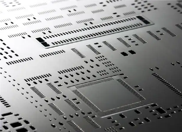
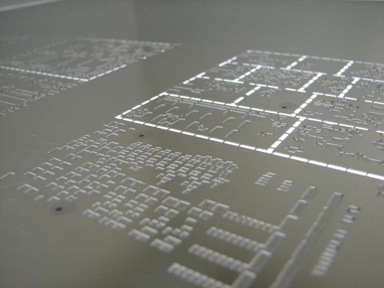
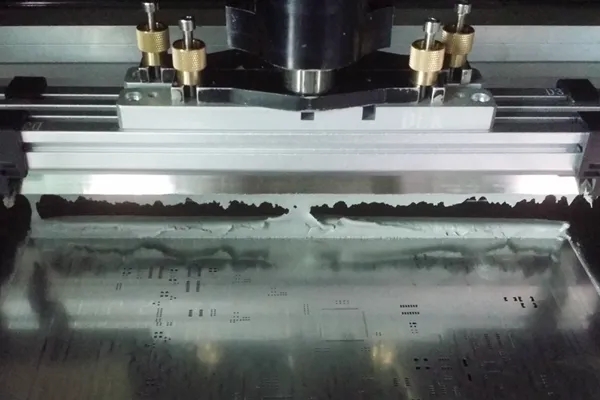
Step Down Stencil: A Guide to Using Frameless vs Frame Stencils
Optimize SMT solder paste processes with step-down stencil design. Compare frameless vs. frame stencils for PCB assembly, focusing on durability, precision, and cost for engineers.
Printed circuit board (PCB) assembly represents a critical phase in electronics manufacturing, where components are mounted onto a board to create functional circuits. This process bridges design and production, ensuring that electronic devices perform reliably in diverse applications. From soldering techniques to component placement, PCB assembly encompasses the methods and technologies that transform bare boards into operational systems. Understanding these elements is essential for engineers, hobbyists, and industry professionals aiming to optimize production efficiency and product quality. Within this category, readers will find a comprehensive collection of guides that detail step-by-step assembly processes, tutorials on advanced tools like surface-mount technology and automated pick-and-place machines, and insights into troubleshooting common issues such as solder joint defects or thermal management challenges. Best practices are highlighted to promote reliability, including strategies for minimizing defects through quality control measures and adhering to industry standards like IPC guidelines. These resources draw from real-world expertise to address both fundamental concepts and cutting-edge innovations in the field. The practical value of mastering PCB assembly extends to numerous sectors, including consumer electronics, automotive systems, medical devices, and aerospace engineering. By applying the knowledge shared here, professionals can reduce manufacturing costs, accelerate time-to-market, and enhance device durability. For instance, effective assembly techniques ensure that circuits withstand environmental stresses, leading to longer-lasting products in demanding conditions. Delving into the articles in this PCB assembly category provides a pathway to deeper technical proficiency. Whether refining prototyping skills or scaling up production, the content equips readers with actionable strategies to tackle real-world challenges and stay ahead in an evolving industry.
Optimize SMT solder paste processes with step-down stencil design. Compare frameless vs. frame stencils for PCB assembly, focusing on durability, precision, and cost for engineers.
Analyze wave soldering and hand soldering for through-hole component assembly. This guide compares process, quality, and cost for engineers selecting optimal PCB manufacturing methods.
Evaluate vacuum and pneumatic ICT fixtures for PCB manufacturing test. This technical guide compares actuation, throughput, and maintenance for test engineering applications.
Optimize reflow soldering for high-yield SMT assembly. This guide covers solder paste, stencil printing, pick-and-place, and thermal profiling for engineers.
Optimize PCB cleaning in mass production: Select equipment, ensure solvent compatibility, validate residues, and minimize environmental impact. Boost reliability with testing and IPC standards—essential for high-yield assembly lines.
Explore the selective soldering process for PCB assembly, covering equipment choices, design considerations, defect identification, and troubleshooting for high-quality results.
Explore essential stencil design principles for surface mount technology (SMT) to ensure precise solder paste application and high-quality PCB assembly.
A comprehensive guide to SMD resistors, covering common sizes like 0603 and 0805, how to read their markings, understand tolerance and wattage, and their diverse uses in modern circuits.
Explore the stamp hole (mouse bites) and V-scoring depanelization methods for PCBs, comparing their advantages, disadvantages, and ideal use cases in manufacturing.
Discover expert USB-C PCB design guidelines for reliable integration, including signal integrity, high-wattage power delivery, EMI mitigation, and layout best practices. Perfect for engineers building next-gen devices.
Unlock ICT advantages in PCB assembly: Achieve high test coverage >95%, precise diagnosis of defects, and customizable verification for operations. Boost yields 98% with IPC-A-610 standards—essential for 2025 wearables and HDI boards.