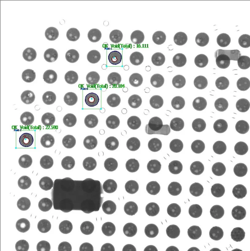
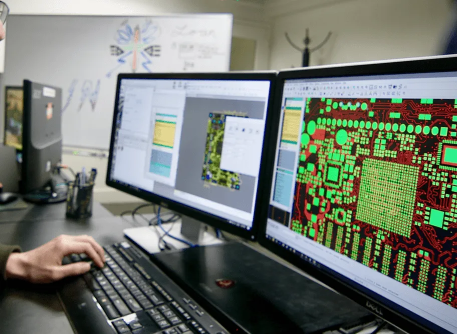
Step Down Stencil: A Guide to Using Frameless vs Frame Stencils
Optimize SMT solder paste processes with step-down stencil design. Compare frameless vs. frame stencils for PCB assembly, focusing on durability, precision, and cost for engineers.
Analyze wave soldering and hand soldering for through-hole component assembly. This guide compares process, quality, and cost for engineers selecting optimal PCB manufacturing methods.
Evaluate vacuum and pneumatic ICT fixtures for PCB manufacturing test. This technical guide compares actuation, throughput, and maintenance for test engineering applications.
Optimize reflow soldering for high-yield SMT assembly. This guide covers solder paste, stencil printing, pick-and-place, and thermal profiling for engineers.
Optimize PCB cleaning in mass production: Select equipment, ensure solvent compatibility, validate residues, and minimize environmental impact. Boost reliability with testing and IPC standards—essential for high-yield assembly lines.
Explore the selective soldering process for PCB assembly, covering equipment choices, design considerations, defect identification, and troubleshooting for high-quality results.
Explore essential stencil design principles for surface mount technology (SMT) to ensure precise solder paste application and high-quality PCB assembly.
A comprehensive guide to SMD resistors, covering common sizes like 0603 and 0805, how to read their markings, understand tolerance and wattage, and their diverse uses in modern circuits.
Explore the stamp hole (mouse bites) and V-scoring depanelization methods for PCBs, comparing their advantages, disadvantages, and ideal use cases in manufacturing.
Explore essential PCB design guidelines for integrating USB-C connectors, focusing on signal integrity, power delivery, and layout best practices for reliable performance.
Unlock ICT advantages in PCB assembly: Achieve high test coverage >95%, precise diagnosis of defects, and customizable verification for operations. Boost yields 98% with IPC-A-610 standards—essential for 2025 wearables and HDI boards.