


PCB Assembly
Printed circuit board (PCB) assembly represents a critical phase in electronics manufacturing, where components are mounted onto a board to create functional circuits. This process bridges design and production, ensuring that electronic devices perform reliably in diverse applications. From soldering techniques to component placement, PCB assembly encompasses the methods and technologies that transform bare boards into operational systems. Understanding these elements is essential for engineers, hobbyists, and industry professionals aiming to optimize production efficiency and product quality. Within this category, readers will find a comprehensive collection of guides that detail step-by-step assembly processes, tutorials on advanced tools like surface-mount technology and automated pick-and-place machines, and insights into troubleshooting common issues such as solder joint defects or thermal management challenges. Best practices are highlighted to promote reliability, including strategies for minimizing defects through quality control measures and adhering to industry standards like IPC guidelines. These resources draw from real-world expertise to address both fundamental concepts and cutting-edge innovations in the field. The practical value of mastering PCB assembly extends to numerous sectors, including consumer electronics, automotive systems, medical devices, and aerospace engineering. By applying the knowledge shared here, professionals can reduce manufacturing costs, accelerate time-to-market, and enhance device durability. For instance, effective assembly techniques ensure that circuits withstand environmental stresses, leading to longer-lasting products in demanding conditions. Delving into the articles in this PCB assembly category provides a pathway to deeper technical proficiency. Whether refining prototyping skills or scaling up production, the content equips readers with actionable strategies to tackle real-world challenges and stay ahead in an evolving industry.
Latest Blogs
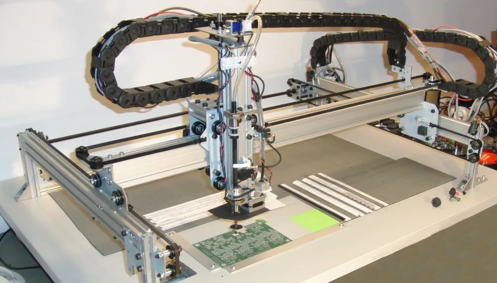
Building a mini pick and place machine for circuit boards
Build a mini DIY pick and place machine with 3D printed parts for custom circuit boards. Guide covers frame assembly, vacuum nozzle, vision system setup, control software, and troubleshooting for electronic hobbyists. Get precise SMD placement and reliable results at home. (198 characters)
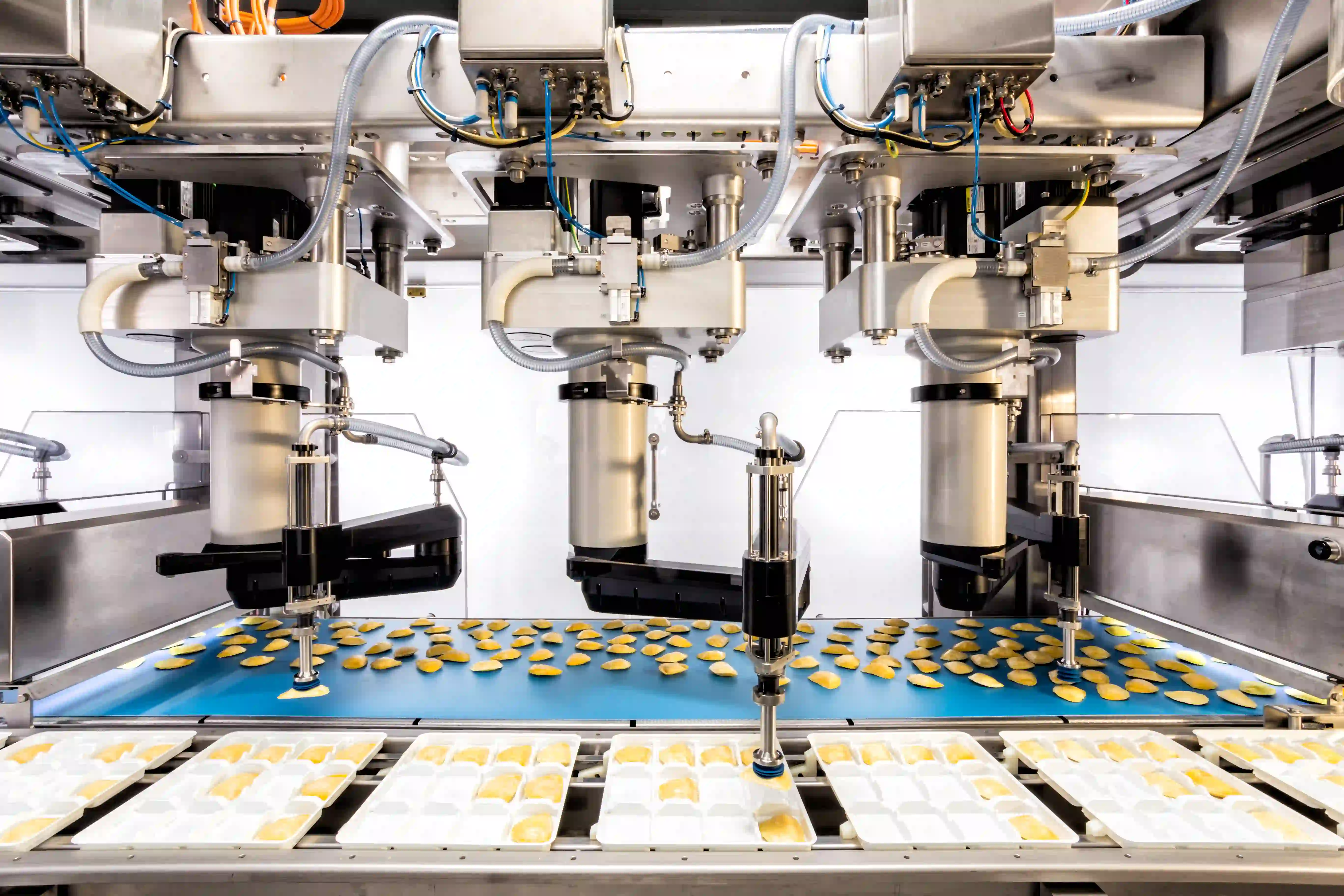
Beginner's Guide to Using Pick and Place Machines for PCB Assembly
Learn how to use PCB pick and place machines for efficient pick and place assembly. This guide covers preparation, operation, reflow soldering, troubleshooting, and best practices for hobbyists building reliable PCBs.
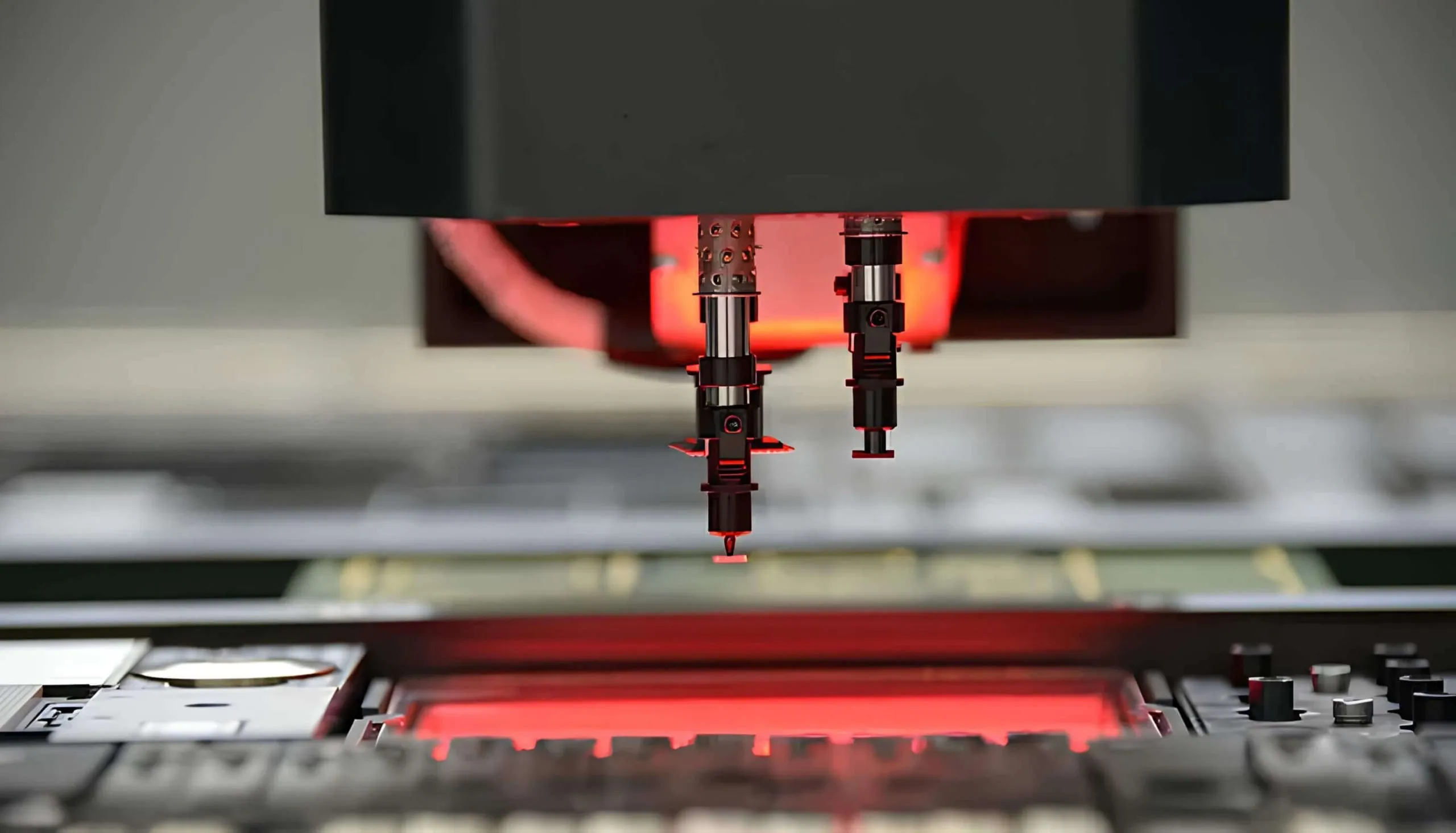
Common Mistakes in the SMT Pick and Place Process
Discover the most common mistakes in the SMT pick and place process — bad nozzles, missing components, feeder failures, and more. Learn practical troubleshooting and prevention strategies to boost yields and reduce downtime in high-volume PCB assembly.
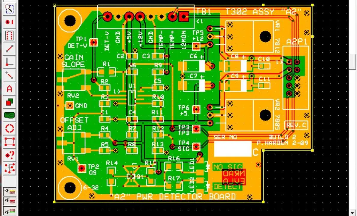
From Schematic to Reality: Assembling Your First Electronic Prototype
Follow this practical guide to electronic prototype assembly, from schematic to soldered board. Beginners learn tools, soldering steps, troubleshooting, and breadboard alternatives for reliable DIY electronics projects and simple circuit builds.
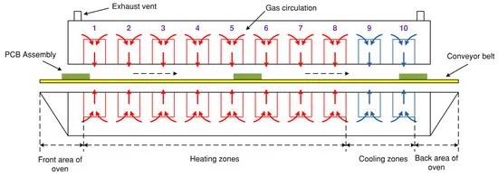
The Impact of PCB Substrate Material on Thermal Performance During SMT Assembly
PCB substrate material shapes thermal performance in SMT assembly by controlling heat dissipation and reflow profiles. Substrate thermal conductivity ensures uniform heating to avoid warpage and voids. Metal core PCBs boost PCB thermal management for high power boards and reliable joints.
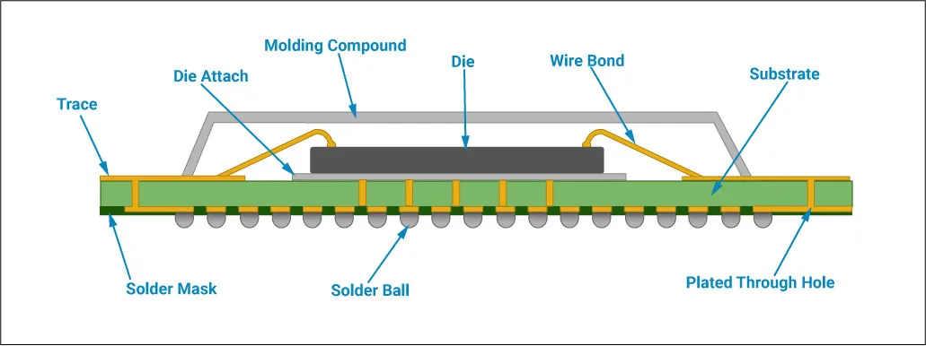
Choosing the Right PCB Substrate for Fine Pitch Component Assembly
Fine pitch BGA substrates need low CTE, warpage control, and HDI compatibility for reliable assembly. Microvia technology supports dense routing, surface finishes boost solderability. Get practical selection criteria, testing methods, and troubleshooting to cut defects and raise yields for engineers.
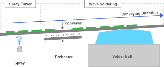
The Impact of Flux on Solder Joint Reliability: Ensuring Long Term Performance
Flux determines solder joint reliability in electronics assembly by enabling wetting while residues risk flux corrosion and weak joints. Practical insights on mechanisms, residue control, best practices, testing, and standards ensure PCB reliability and strong joint performance over time.
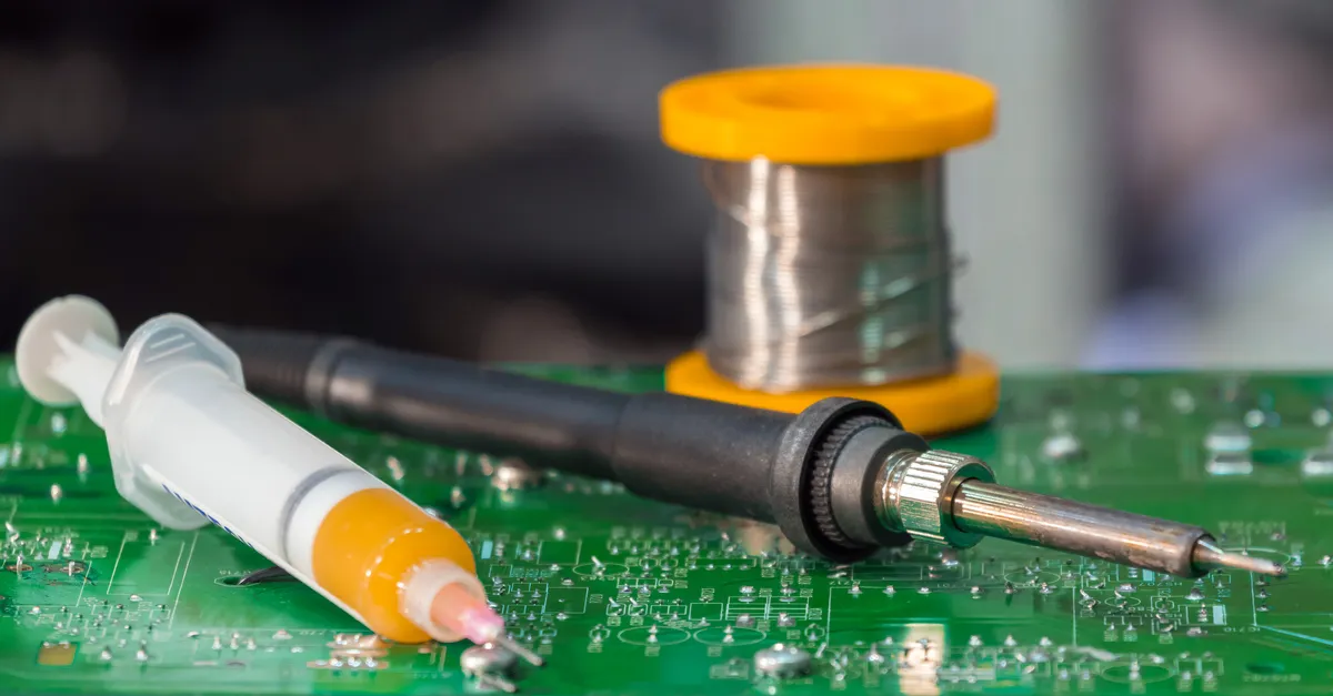
Mastering Flux Selection: A Comprehensive Guide for Optimal Assembly
Flux selection guide for PCB assembly covers types like no-clean and water-soluble, choosing the right flux for SMT and through-hole, compatibility factors, and best practices. Practical tips ensure reliable joints, minimize defects, and improve yields for electric engineers in production.
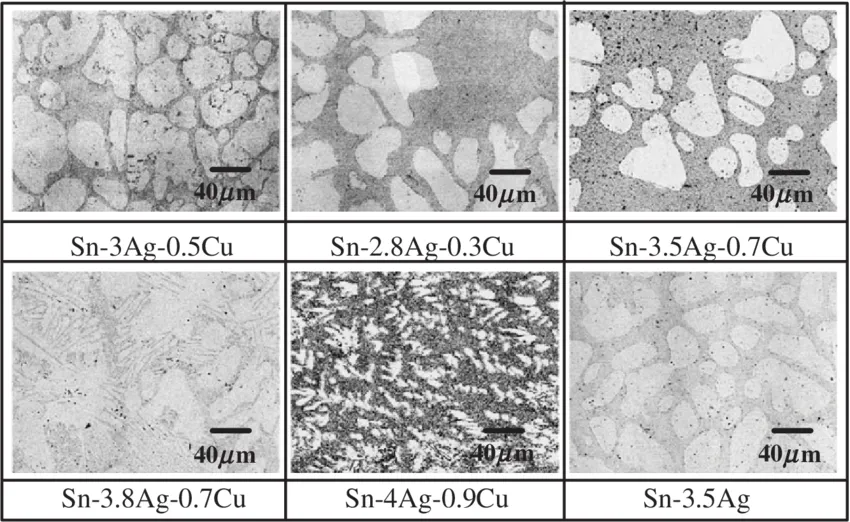
The Ultimate Guide to Leaded Solder Alloys: Choosing the Right Mix for Your PCB Assembly
This leaded solder alloy chart covers compositions, melting temperatures, and tensile strength for PCB assembly. Pick the best leaded solder for wave soldering with Sn63Pb37 or reflow with SnPbAg alloys. Essential composition guide helps electric engineers achieve reliable joints and fewer defects.
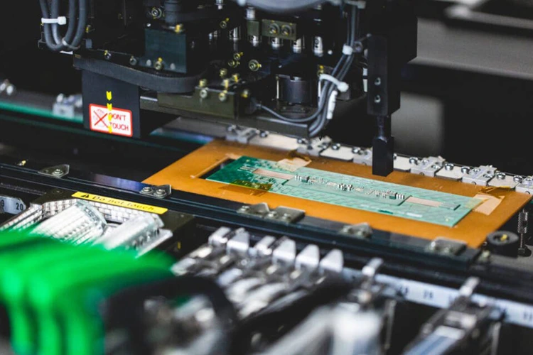
Unlocking Reliability: Why Leaded Solder Still Reigns Supreme in Aerospace PCBs
Aerospace and defense still rely on leaded solder for unmatched ductility, fatigue resistance, and long-term reliability under extreme conditions. This guide compares leaded vs lead-free performance, details regulatory exemptions, best practices, and real-world case studies.
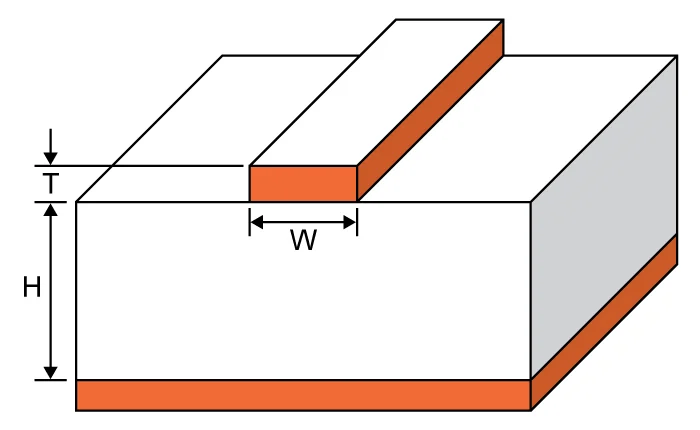
Enhancing Signal Integrity in High Speed PCB Designs
Maintain signal integrity in high-speed PCB designs using impedance control, trace routing, termination techniques, ground planes, and decoupling capacitors. Practical strategies for engineers to reduce reflections, crosstalk, noise, and ensure reliable data transmission at gigabit speeds.
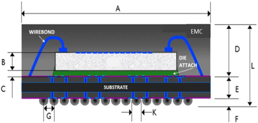
A Comprehensive Guide to BGA Assembly and Inspection
Master BGA assembly and inspection with this step-by-step SMT guide. Learn solder paste printing, reflow profiling, X-ray techniques, rework procedures, and troubleshooting for reliable high-density PCB joints. Boost yield and quality today.


