Introduction
Printed circuit board (PCB) schematics serve as the blueprint for any electronic circuit, showing how components connect logically rather than their physical placement. For electronic hobbyists, mastering PCB schematic reading unlocks the ability to troubleshoot, modify, and understand devices without guesswork. This guide focuses on practical steps for understanding PCB schematics, from recognizing symbols to tracing circuits for fault finding. Whether repairing a gadget or prototyping a project, effective diagnostics start with interpreting these diagrams accurately. By following structured techniques, hobbyists can save time and avoid common pitfalls in circuit analysis.
What Is a PCB Schematic and Why It Matters
A PCB schematic is a symbolic representation of an electronic circuit, illustrating electrical connections between components using standardized lines and symbols. Unlike the physical PCB layout, which shows the actual board traces and component positions, the schematic prioritizes logical flow for easier comprehension. This distinction between PCB layout vs schematic is crucial for diagnostics, as schematics reveal intended functionality while layouts depict manufacturing realities. Hobbyists rely on schematics for initial fault finding with schematics, identifying potential issues like open circuits or shorts before probing the board. Understanding PCB schematics ensures compliance with design principles outlined in standards like IPC-2221, which guides overall circuit board design practices.
In practice, schematics matter because they provide a high-level view that speeds up problem-solving. For instance, when a device fails, the schematic helps pinpoint power paths or signal routes quickly. Hobbyists often encounter multi-page schematics in complex projects, making systematic reading essential. Ignoring the schematic leads to inefficient trial-and-error testing, which can damage components.
Key Schematic Symbols Every Hobbyist Should Know
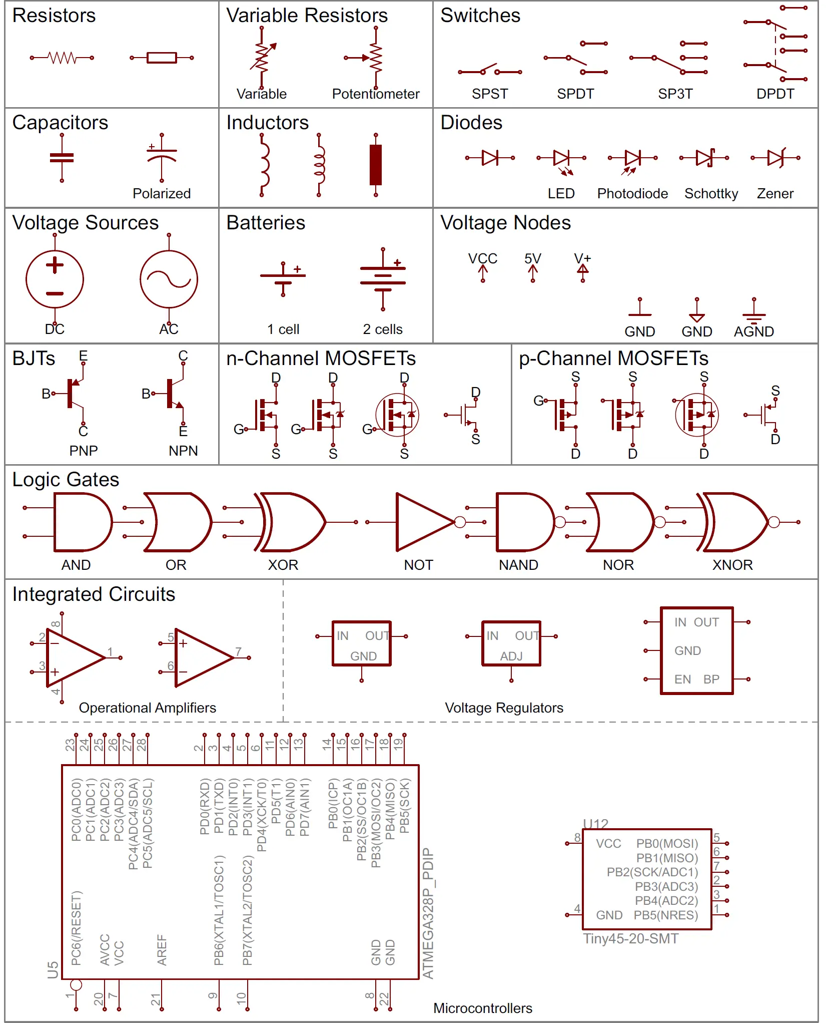
Schematic symbols represent components universally, allowing quick identification across diagrams. Common passive components include the resistor, shown as a zigzag line or rectangle, the capacitor as two parallel lines, and the inductor as a series of loops. Active components like transistors appear as arrows indicating current flow direction, while integrated circuits (ICs) are rectangles with numbered pins. Diodes feature a triangle with a bar, symbolizing one-way current, and switches use lines with gaps for open or closed states. Standards such as IPC-2612-1 define guidelines for generating these electronic symbols for circuit diagrams, ensuring consistency.
Power and ground symbols simplify large diagrams; a horizontal line often denotes ground, while arrows or circles indicate voltage sources. Connectors and test points use simple dot junctions or labeled pins. Hobbyists benefit from memorizing these for faster PCB schematic reading. Variations exist, but core shapes remain standard across most designs.
Common Schematic Symbols Table
| Component | Symbol Description | Common Variations | Typical Use / Notes |
|---|---|---|---|
| Resistor | Zigzag line or rectangle | Box with value | Current limiting, pull-ups |
| Capacitor | Two parallel lines | Polarized = + sign | Filtering, decoupling |
| Inductor | Series of loops or coils | Iron core = lines through loops | Filtering, oscillators |
| Diode | Triangle pointing to a line | LED = arrows added | Rectification, protection |
| LED | Diode symbol with arrows emitting light | Different colors in documentation | Indicators, displays |
| Transistor (NPN) | Circle with arrow pointing out from base | BJT vs MOSFET variants | Switching, amplification |
| IC / Op-Amp | Triangle or rectangle with pin numbers | Power pins often shown separately | Amplifiers, microcontrollers |
| Ground | Three decreasing horizontal lines | Chassis vs signal ground | Reference point |
| Power / VCC | Circle with + or labeled voltage | Arrow pointing up | Supply rails |
| Switch | Two lines with a break or angled line | Pushbutton, toggle, relay | User input, power control |
Mastering Circuit Tracing in Schematics
Circuit tracing involves following signal paths from input to output using net labels, reference designators, and connection lines. Start at power entry points, noting voltage rails and their distribution to components. Junction dots indicate wire crossings with connections, while lines without dots mean no connection. Reference designators like R1 or C5 link symbols to the bill of materials and physical board locations. For complex circuits, use hierarchical sheets or buses to group signals efficiently.
Effective tracing aids in understanding PCB schematics by revealing current flow and potential bottlenecks. Hobbyists can mark paths with colored highlighters on printouts for clarity. When tracing feedback loops or oscillators, note component values to verify operation. This method directly supports fault finding with schematics, isolating issues like missing bypass capacitors.
Practice on simple power supplies first, progressing to amplifiers. Tools like multimeters confirm traces on the actual board. Tracing builds intuition for interpreting PCB diagrams holistically.
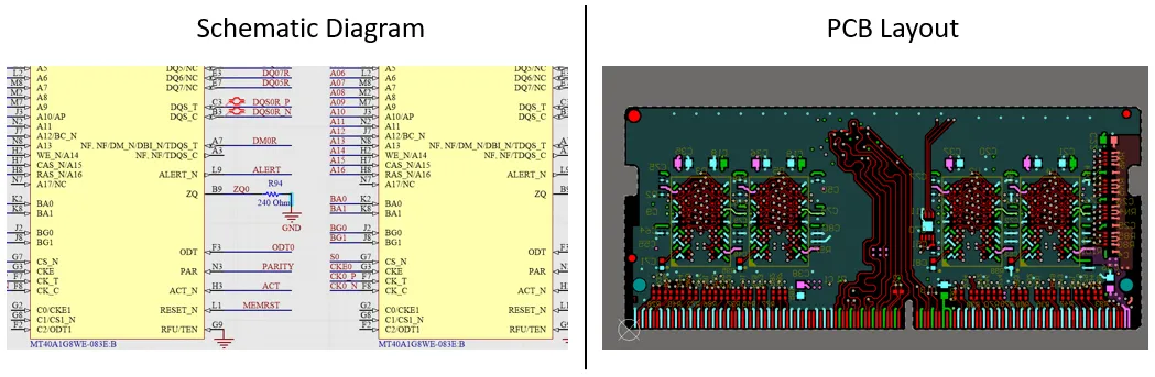
PCB Layout vs Schematic: Navigating the Differences
The PCB layout translates the schematic into a physical board, routing traces between pads while considering factors like signal integrity and thermal management. Schematics ignore physical constraints, focusing purely on connectivity, whereas layouts optimize for manufacturability and performance. Misalignments occur if layout changes alter schematic intent, such as rerouted grounds causing noise. Hobbyists must cross-reference both for accurate diagnostics, using the schematic for logic and layout for measurements. Cross-referencing both is essential for accurate repairs—see our practical guide on troubleshooting common errors in PCB schematic design.
Key differences include trace lengths, via placements, and layer stacking, absent in schematics. Understanding PCB layout vs schematic prevents confusion during repairs. For example, a schematic might show a direct connection, but the layout uses vias across layers. Standards like IPC-2221 address these transitions in design.
Hobbyists often view Gerber files or board images alongside schematics. This dual approach enhances circuit tracing on real hardware. Recognizing layout variations improves overall fault finding efficiency.
Step-by-Step Guide to Reading and Tracing Circuits
Follow this repeatable workflow for reliable PCB schematic reading:
- Identify Power and Ground — Locate the main voltage rails (VCC, 5V, 3.3V, GND). Mark them with color (red for positive, black/green for ground).
- Locate Major Functional Blocks — Group components into power supply, microcontroller, sensors, drivers, etc.
- Trace Signal Flow — Start from inputs and follow net labels or lines to outputs. Note junction dots (connection) versus crossing lines (no connection).
- Check Reference Designators — Match every symbol to its physical counterpart on the board.
- Verify Expected Values — Note typical voltages, frequencies, or logic levels next to key test points.
- Document as You Go — Annotate a printed or digital copy with measurements and observations.
This power-first method quickly reveals whether the problem is in the supply, a specific block, or a signal path. Practice on simple single-sheet designs (e.g., Arduino Nano schematic) before moving to complex multi-page diagrams.
Fault Finding with Schematics: Step-by-Step Approach
Begin fault finding with schematics by verifying power supply integrity from the input to critical rails. Check for obvious discrepancies like missing components or incorrect polarities using reference designators. Trace suspect signals step-by-step, calculating expected voltages with Ohm's law for passives. Isolate sections by injecting test signals or lifting pins temporarily.
Divide-and-conquer narrows issues: power off sections mentally via the schematic. Common faults include solder bridges mimicking shorts or cracked traces breaking paths. Visual inspection pairs with schematic knowledge for targeted probing. Interpreting PCB diagrams this way minimizes risks to working parts. These techniques work best when combined with modern tools—explore them in our overview of PCB schematic tools for prototyping and diagnostics.
Document findings with notes on the schematic printout. Recheck traces after fixes to confirm resolution. This systematic process turns hobbyist diagnostics into reliable skills.
Best Practices for Interpreting PCB Diagrams
Print schematics at full size for annotations and use consistent lighting for readability. Organize multi-page diagrams by function, like power, analog, and digital blocks. Cross-reference with datasheets for unfamiliar symbols or IC pinouts. Maintain a glossary of custom net names for reuse in projects.
Adhere to standards for symbol clarity, as per IPC-2612-1, to avoid misinterpretation. Zoom tools in PDF viewers aid detailed inspection. Practice on open-source projects to build speed. Combine with oscilloscope captures for dynamic verification. For application-specific examples, review our detailed walkthrough on decoding security camera PCB schematics.
Regular review reinforces PCB schematic reading proficiency. Share annotated diagrams in hobbyist communities for feedback. These habits elevate diagnostics from basic to expert level.
Real-World Examples and Hobbyist Case Studies
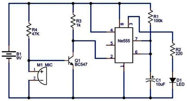
Case 1: Simple 555 Timer Circuit
Symptom: No oscillation. Schematic tracing revealed missing connection dot on the discharge pin. Fixed in 5 minutes after visual confirmation on the board.
Case 2: Audio Amplifier Repair
Symptom: Distorted output. Schematic showed expected 12 V at the op-amp supply, but measurement revealed only 4.2 V due to a cracked trace on the power rail. Layout cross-reference located the exact failure point.
Case 3: USB Charger Diagnosis
Schematic-guided voltage measurements quickly isolated a failed feedback resistor on the switching regulator, preventing unnecessary replacement of the main IC.
These examples demonstrate how systematic PCB schematic reading turns random probing into targeted, efficient repairs.
Advanced Tips – Hierarchical Schematics, Simulation, and Annotation
Modern schematics are often hierarchical, with top-level blocks linking to detailed sub-sheets. Learn to navigate hierarchy trees and understand bus notation for high-pin-count devices.
Integrate simulation early. Tools like LTspice or the built-in KiCad simulator let you verify expected behavior directly from the schematic before ordering boards. Annotate simulations with expected waveforms for later comparison during physical debugging.
Good annotation habits—adding test-point labels, expected voltage notes, and revision history—make future diagnostics significantly easier. Treat your annotated schematic as living documentation.
Conclusion
Decoding PCB schematics empowers electronic hobbyists with the tools for precise diagnostics and creative modifications. From grasping schematic symbols to advanced circuit tracing, these skills bridge theory and practice effectively. Recognizing differences between PCB layout vs schematic prevents costly errors in fault finding. Consistent application of best practices, aligned with industry standards, ensures reliable results. Start with simple circuits and progress, turning every project into a learning opportunity.
FAQs
Q1: How do I start PCB schematic reading as a beginner?
A1: Begin with basic components like resistors and capacitors, using common schematic symbols as references. Follow power paths first, then trace signals using net labels. Practice on single-sheet diagrams to build confidence in understanding PCB schematics. This foundation supports circuit tracing and fault finding with schematics quickly.
Q2: What is the main difference in PCB layout vs schematic?
A2: Schematics show logical connections symbolically, while layouts depict physical traces and placements. Schematics aid interpreting PCB diagrams for functionality, but layouts reveal real-world routing issues. Use both for comprehensive diagnostics in hobby projects.
Q3: Why are schematic symbols standardized?
A3: Standards like IPC-2612-1 ensure universal recognition of symbols across diagrams, facilitating PCB schematic reading globally. This consistency speeds up understanding PCB schematics and reduces errors in circuit tracing for hobbyists and pros alike.
Q4: How does fault finding with schematics save time?
A4: Schematics guide targeted probing by highlighting expected paths, avoiding random checks. Prioritize power rails and key signals for quick isolation of faults. This method outperforms blind measurements, enhancing efficiency in interpreting PCB diagrams.
References
IPC-2221A — Generic Standard on Printed Board Design. IPC.
IPC-2612-1 — Electronic Symbols for Circuit Diagrams. IPC.