Introduction
Turning a circuit idea into a functional printed circuit board starts with a clear PCB design workflow tutorial. For electronic hobbyists, this process bridges the gap between conceptual sketches and real-world prototypes. It involves several interconnected steps, from capturing the schematic to generating files ready for manufacturing. Understanding this workflow helps avoid common mistakes and ensures your boards work as intended. In this guide, we break it down into manageable phases, tailored for beginners eager to build their first custom PCB. By the end, you will grasp the essentials of schematic capture, PCB layout basics, creating a bill of materials, and Gerber file generation for beginners.
Why the Typical PCB Design Workflow Steps Matter for Hobbyists
The PCB design workflow provides a structured path that minimizes errors and optimizes board performance. Hobbyists often jump straight to wiring breadboards, but PCBs offer reliability, compactness, and repeatability for projects like Arduino shields or sensor modules. A well-defined workflow aligns component placement with signal integrity needs, reducing noise and failures during testing. It also prepares files that manufacturers can process without revisions, saving time and cost. Following this sequence fosters good habits, making complex designs approachable over time. Ultimately, mastering the workflow empowers hobbyists to iterate faster and achieve professional results.
Step 1: Schematic Capture Basics
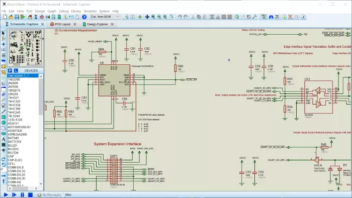
Schematic capture forms the foundation of any PCB design workflow tutorial by visually representing the electrical connections. Begin by selecting components from libraries, such as resistors, capacitors, and microcontrollers, and placing them on the canvas. Draw nets to connect pins logically, ensuring power rails and ground planes are clearly defined. Add reference designators like R1 or C5 for easy tracking. Annotate values and tolerances to match your project specs. This phase verifies circuit functionality through simulation if available, catching logic errors early.
Hobbyists benefit from hierarchical schematics for larger projects, breaking them into sub-circuits for clarity. Pay attention to decoupling capacitors near ICs to stabilize power. Once complete, perform an electrical rule check to flag unconnected pins or shorts. Export the netlist, which lists all connections, for the next step. Schematic capture sets the tone for efficient PCB layout basics ahead.
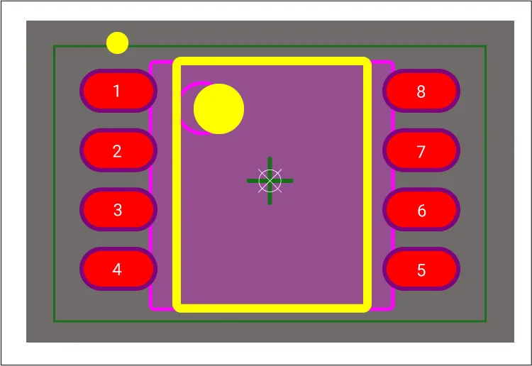
Step 2: Component Library and Footprint Assignment
After schematic capture, assign footprints to each component, linking electrical symbols to physical packages. Footprints define pad sizes, shapes, and spacing based on manufacturer datasheets. Common types include through-hole for prototypes and surface-mount for dense boards. Mismatch here leads to assembly issues, so double-check dimensions like lead pitch and body size. Libraries often include standard footprints, but custom ones may be needed for unique parts. This step ensures the netlist translates accurately to the physical layout.
Guidelines from IPC-7351 help standardize land patterns for reliable soldering. Hobbyists should prioritize 0805 or 1206 SMD sizes for hand-soldering ease. Verify polarity for diodes and electrolytics to avoid reversal during placement. Once assigned, update the schematic to reflect changes. This preparation smooths the transition to PCB layout basics.
Step 3: PCB Layout Basics
PCB layout basics transform the netlist into a routable board outline. Start by defining the board shape, layers, and stackup, typically single or double-sided for beginner projects. Place components strategically: high-speed signals near each other, connectors at edges, and heat-generating parts with clearance. Maintain minimum clearances for traces and vias per your chosen technology. Route traces manually or autoroute, prioritizing short paths for critical nets. Add silkscreen for labels and fiducials for alignment.
Layer assignment matters: signals on top, ground plane on bottom for shielding. Follow design rules for trace width, calculated by current needs, to prevent overheating. Vias connect layers efficiently, but minimize their use in simple designs. After routing, run design rule checks for violations like spacing errors. Iterate until clean, then generate a preview. This phase embodies PCB layout basics in the full workflow.
Suggested Reading: PCB Layout: Ensuring Signal Integrity in Mixed Signal Designs
Step 4: Creating a Bill of Materials (BOM)
Creating a bill of materials streamlines procurement and assembly in the PCB design workflow tutorial. The BOM lists every component with reference designator, value, footprint, manufacturer part number, and quantity. Export it from your design environment as a CSV for editing in spreadsheets. Include package details and supplier notes for sourcing. Group identical parts to reduce variants and cost. A complete BOM prevents shortages during prototyping.
Hobbyists often source from distributors, so add tolerances and voltage ratings for alternatives. Format columns clearly: Designator, Footprint, Value, Qty, Description. Review for duplicates or missing passives. Integrate it with pick-and-place files later. This step ensures all parts align with schematic capture outputs.
Step 5: Design Rule Checks and Optimization
Before finalizing, perform comprehensive design rule checks across the board. These verify trace widths, clearances, via sizes, and netlist integrity against predefined rules. Adjust parameters for your fab house capabilities, like minimum trace 6 mil for standard processes. Fix violations iteratively, rerouting as needed. Simulate for signal integrity if advanced tools allow. Optimization includes adding test points and mounting holes.
Adhering to IPC-2221 guidelines for trace spacing enhances reliability under voltage stress. Hobbyists should enable checks for annular ring and drill sizes. Document any waivers with justification. A clean DRC report confirms readiness for output files.
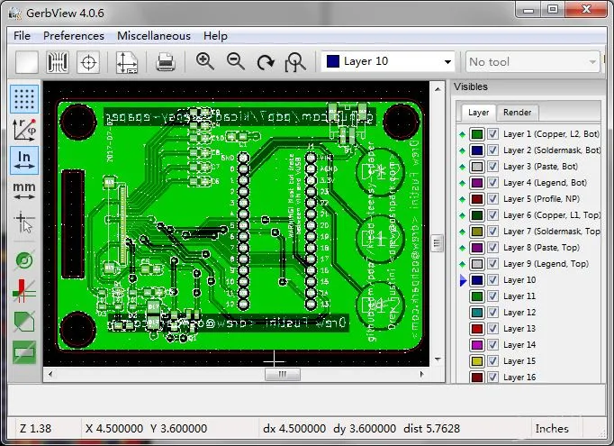
Step 6: Gerber File Generation for Beginners
Gerber file generation for beginners caps the workflow by producing manufacturing-ready data. Generate separate Gerbers for each layer: copper top/bottom, soldermask, silkscreen, and outline. Include drill files in Excellon format for vias and holes. Output panelization if multiple boards fit a panel. Verify files in a free viewer for overlaps or missing data. Zip all together with a readme specifying stackup and finishes.
Standards like Gerber RS-274X ensure compatibility across fabricators. Name files logically: top_copper.gbr, bottom_solder.gtl. Include fabrication notes on finish like HASL or ENIG, and solder mask color. Test plot to confirm. This step completes Gerber file generation for beginners.
Suggested Reading: Gerber Files Unveiled: Understanding and Generating Gerber Files for PCB Manufacturing
Best Practices for Typical PCB Design Workflow Steps
Throughout the PCB design workflow tutorial, maintain version control by saving iterations. Use consistent naming for files and layers to avoid confusion. Collaborate with checklists: netlist match, BOM accuracy, DRC pass. For hobbyists, start small with 2-layer boards under 100x100mm. Simulate early to validate functionality. Document decisions for future revisions.
Incorporate thermal reliefs on pads for easier soldering. Space components for probe access during testing. Review stackup for impedance control if signals exceed 50MHz. These practices elevate schematic capture and PCB layout basics.
Common Pitfalls in Main PCB Design Workflow Steps
Beginners often overlook netlist mismatches between schematic and layout, causing opens or shorts. Solution: Forward annotate after changes. Overcrowded routing leads to DRC fails; simplify by repositioning. BOM errors like wrong footprints delay builds; cross-verify datasheets. Gerber omissions, such as missing paste layer for SMT, frustrate fabs; always checklist outputs.
Power plane splits create inductance; use solid pours where possible. Ignoring fab limits on aspect ratio results in drill breaks. Troubleshoot with 3D renders for height clearance. Patience in iterations pays off.
Conclusion
The PCB design workflow tutorial from schematic capture to Gerber file generation equips hobbyists with a repeatable process for success. Each step, from PCB layout basics to creating a bill of materials, builds reliability into your projects. Embrace standards for quality, iterate thoughtfully, and test prototypes rigorously. As you gain experience, scale to multi-layer boards and high-speed designs. This guide serves as your starting point toward professional-grade electronics. Start your next project today and see the workflow in action.
FAQs
Q1: What is schematic capture in a PCB design workflow tutorial?
A1: Schematic capture involves drawing the circuit diagram with symbols for components and lines for connections. It generates a netlist for layout. Beginners place parts logically, add values, and check for errors. This step ensures electrical design integrity before physical placement. Mastering it simplifies PCB layout basics ahead.
Q2: How do PCB layout basics affect board performance?
A2: PCB layout basics determine signal quality, heat dissipation, and manufacturability. Proper component placement minimizes noise, while trace routing controls impedance. Follow clearances to prevent shorts. Hobbyists focus on short paths for analog signals. Run DRC to validate. Good layout reduces troubleshooting time.
Q3: Why is creating a bill of materials essential for beginners?
A3: Creating a bill of materials lists all parts needed, preventing sourcing delays. It includes quantities, footprints, and descriptions for ordering. Export from design tools and edit for suppliers. Accurate BOM supports Gerber file generation for beginners. It streamlines assembly too.
Q4: What should beginners know about Gerber file generation?
A4: Gerber file generation creates layer-specific files for fabrication, like copper and drill data. Verify in viewers before zipping. Specify finishes and tolerances in notes. It follows the full PCB design workflow tutorial. Common errors include missing layers; checklist prevents them.
References
IPC-2221B - Generic Standard on Printed Board Design. IPC, 2009
IPC-7351C - Generic Requirements for Surface Mount Design and Land Pattern Standard. IPC, 2010