Introduction
High-speed signals in modern PCBs operate at frequencies exceeding several gigahertz, where even minor timing variations can compromise system performance. Jitter, a key metric in high-speed signal integrity, represents these timing deviations that accumulate and degrade data transmission quality. Electrical engineers designing PCBs for applications like telecommunications, computing, and data centers must prioritize PCB layout best practices to mitigate jitter effectively. This article explores PCB jitter reduction methods, delving into causes, technical principles, and actionable strategies for clock signal jitter and other high-speed interfaces. By mastering these techniques, designers can ensure robust signal timing errors minimization and reliable operation. Understanding jitter control not only enhances product reliability but also aligns with industry demands for ever-faster data rates.
What Is Jitter and Why It Matters for High-Speed Signals
Jitter refers to the deviation in the timing of signal edges from their ideal positions, manifesting as short-term variations in signal periodicity. In high-speed PCBs, it directly impacts eye diagram quality, where excessive jitter closes the eye opening and increases bit error rates. Engineers classify jitter into random jitter from noise sources and deterministic jitter from systematic effects like reflections. Clock signal jitter, in particular, propagates through the system, affecting downstream receivers and synchronization. For signals above 1 Gbps, even picosecond-level jitter can lead to setup and hold violations, causing intermittent failures. Adhering to PCB layout best practices for jitter control is essential to maintain signal integrity across multi-layer boards.
The relevance of jitter control extends to compliance with performance specifications in demanding environments. In data converters or serdes interfaces, total jitter budgets dictate the maximum allowable deviation for error-free operation. Without proper management, signal timing errors amplify through cascading effects, reducing margins for process variations and temperature drifts. Engineers must quantify jitter using metrics like peak-to-peak or RMS values to predict system behavior accurately.
Fundamental Causes of Jitter in PCB Layouts
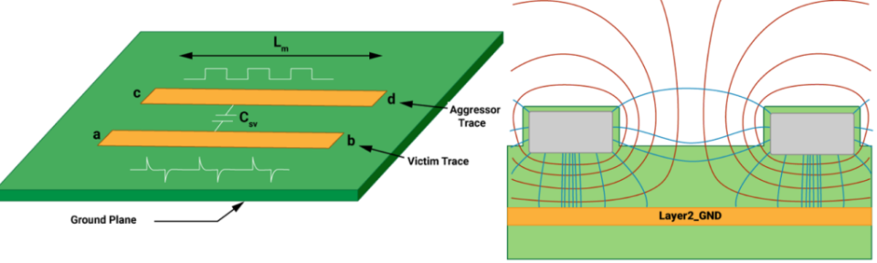
Jitter arises primarily from impedance discontinuities that cause reflections, introducing deterministic jitter components. Crosstalk between adjacent traces couples noise, adding periodic jitter modulated by switching patterns. Intersymbol interference occurs when previous bits distort current edges due to unterminated lines or dispersive dielectrics. Power supply noise couples into signals via inadequate decoupling, contributing to random jitter. Vias and bends further exacerbate these issues by altering characteristic impedance and introducing stubs.
Clock distribution networks amplify jitter through fanout and skew mismatches across branches. Ground bounce from simultaneous switching generates return path interruptions, injecting bounded jitter. Dielectric losses in FR-4 materials at high frequencies cause signal attenuation and phase shifts, worsening timing errors. Identifying these mechanisms requires time-domain reflectometry and eye pattern analysis during design verification.
Technical Principles Behind Jitter Generation and Propagation
Transmission line theory governs high-speed signal behavior, where signals propagate as guided waves between conductors and reference planes. Characteristic impedance mismatch leads to reflections quantified by the reflection coefficient, directly correlating to deterministic jitter amplitude. Crosstalk voltage follows capacitive and inductive coupling models, with near-end and far-end components peaking at specific trace separations. Random jitter stems from thermal noise in resistors and shot noise in drivers, following Gaussian distributions.
Dielectric constant variations across the stackup introduce propagation delay skew, manifesting as static phase jitter. Vias act as lumped discontinuities, modeled as series inductance and shunt capacitance, which ring at resonant frequencies. Power integrity interactions, such as simultaneous switching noise, modulate supply rails and inject bounded jitter via substrate coupling. Engineers apply these principles using field solvers to predict jitter contributions pre-layout.
PCB Jitter Reduction Methods: Stackup and Material Selection
Optimal stackup design forms the foundation of high-speed signal integrity, ensuring symmetric layers to minimize warpage and maintain plane capacitance. Place high-speed signals adjacent to continuous reference planes, typically ground, to provide low-inductance return paths and reduce loop inductance. Core and prepreg selection influences dielectric constant uniformity, critical for consistent propagation delays. IPC-2221 guidelines recommend calculating trace widths and spacing based on target impedance, usually 50 ohms single-ended or 100 ohms differential. These choices align with our comprehensive guide to optimizing PCB stack up for high speed signals.
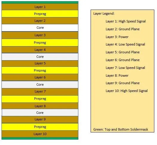
Thinner dielectrics enhance coupling, suppressing common-mode noise and deterministic jitter from imbalances. Avoid splitting planes under signal traces to prevent return path detours that increase jitter. Material choices with low loss tangents, like those specified in performance classes, further aid clock signal jitter minimization.
Routing Strategies for Minimizing Signal Timing Errors
Length matching ensures skew-free arrival times for differential pairs and clock nets, using serpentine or trombone patterns within tolerances of 0.5 mm or less. Route high-speed signals on inner layers away from edges to avoid fringing fields, and use 45-degree bends instead of 90-degree corners to reduce reflections. Minimize via count by optimizing pin assignments, and employ backdrilled vias to stub-stub ends below signal bandwidth. Guard traces or stitching vias shield sensitive nets from crosstalk. Proper implementation also benefits from our detailed best practices on mastering differential pair routing for high-speed PCB design.
Maintain minimum spacing per coupling models, often 3-5 times trace width, to keep far-end crosstalk below 1% of signal amplitude. For clock trees, H-tree or balanced fanout topologies equalize delays. These PCB layout best practices directly target deterministic jitter sources.
Power Integrity Techniques to Combat Jitter
Decoupling capacitors placed within 1 cm of drivers and receivers shunt high-frequency noise, stabilizing supplies and reducing random jitter. Use arrays of low-ESL ceramics spanning frequencies from 10 MHz to 10 GHz. Dedicated power planes with interplane capacitance suppress ground bounce. Via fences along plane edges contain slot resonances that couple noise.
Bulk capacitance near voltage regulators handles low-frequency transients. PDN impedance targets below 10 mohm up to Nyquist frequency minimize supply-induced jitter. These measures integrate seamlessly with signal routing for holistic high-speed signal integrity. For deeper insight into return paths, see our companion article on mastering PCB ground plane design for high-speed signal integrity.
Via and Transition Optimization
Blind and buried vias reduce stub lengths, preserving impedance continuity and slashing via-induced jitter. Staggered via patterns in dense areas avoid anti-pads resonance. Controlled drill sizes per IPC standards ensure plating uniformity, minimizing barrel inductance. Signal launch optimization at connectors matches transition impedances.
Simulation Tools for Jitter Prediction and Analysis
Pre-layout and post-layout simulation are essential for PCB jitter control. Keysight ADS, Siemens HyperLynx, and Cadence Sigrity are industry standards. Use S-parameter models of the channel combined with IBIS-AMI transmitter/receiver models to predict eye diagrams and bathtub curves. Run Monte Carlo analysis to account for manufacturing variation. These tools can separate RJ and DJ contributions and optimize routing before tape-out, often reducing measured jitter by 30–50%.
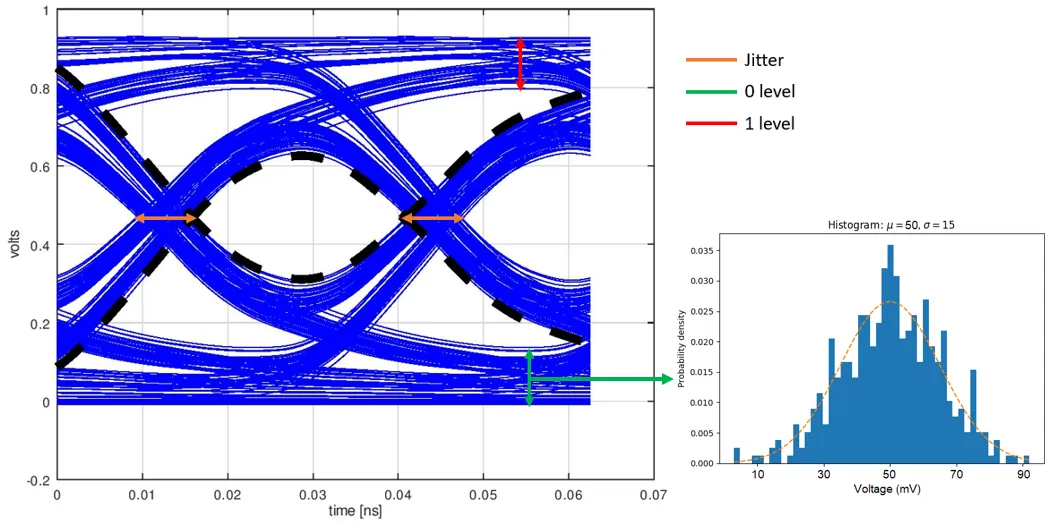
Eye Diagram Analysis and Jitter Measurement Techniques
The eye diagram provides a comprehensive visual summary of jitter and noise. Generate it using a real-time oscilloscope or BERT with pattern trigger. Measure eye height, eye width, and eye crossing percentage at the receiver. Advanced scopes separate random and deterministic jitter using RJ/DJ extrapolation or TIE (Time Interval Error) analysis over 10⁶–10⁸ cycles.
Typical scope settings for 32 Gbps signals include 50 GS/s sampling, minimal bandwidth limiting, and compliance masks per the relevant standard (PCIe, USB, Ethernet). A healthy eye at 32 Gbps should show >30% UI horizontal opening and adequate vertical margin after equalization.
Verification and Analysis Approaches
Pre-layout simulations using S-parameters predict jitter budgets, allocating margins for fabrication tolerances. Post-layout extraction feeds IBIS models into timing analysis for total jitter estimation. Eye diagram metrics like height and width quantify margins against bathtubs curves. TDR confirms impedance profiles.
JESD65B definitions standardize jitter measurements, such as cycle-to-cycle and period jitter over thousands of cycles. Board-level testing with oscilloscopes validates designs.
Troubleshooting Common Jitter Issues
Excessive deterministic jitter often traces to unterminated stubs or plane splits; inspect via stubs and reroute returns. Random jitter spikes indicate PDN weaknesses; add decoupling iteratively. Skew in clocks points to unmatched lengths; apply tuning tools. Eye closure from ISI requires equalization or pre-emphasis at drivers.
Fabrication variations like etch tolerances demand guardbanding. Iterative prototyping refines layouts.
Table: Enhanced Troubleshooting Matrix for Jitter Problems
| Symptom | Likely Root Cause | IPC / Standard Reference | Diagnostic Method | Corrective Action |
|---|---|---|---|---|
| Excessive DJ, closed eye | Via stubs or impedance mismatch | IPC-6012 §3.6, PCIe spec | TDR + eye diagram | Back-drill vias, optimize transitions, add termination |
| High RJ, noisy eye | PDN resonance or insufficient decoupling | IPC-2152, JESD65B | PDN impedance scan, scope FFT | Add/decouple capacitors, improve plane continuity |
| Periodic jitter spikes | Crosstalk or fiber weave skew | IPC-2221B | Near/far-end crosstalk measurement | Increase spacing, change routing layer, use low-Dk material |
| Skew-induced DJ | Unmatched lengths or asymmetric stackup | JESD65B | Length report + simulation | Apply tuning, enforce symmetric stackup |
Jitter Budget Allocation for Modern High-Speed Interfaces
Modern interfaces require explicit jitter budgets:
- PCIe 5.0/6.0: Total jitter < 0.5 UI at 10⁻¹² BER; RJ typically allocated < 0.2 UI.
- DDR5: Write/Read clock jitter < 5–8 ps RMS; tight DQ-DQS skew budgets.
- 112G SerDes (Ethernet/Optical): Total integrated jitter often < 150 fs RMS for PAM4 signaling.
Allocate approximately 30% of the budget to transmitter, 40% to channel (PCB + package), and 30% to receiver. Use simulation to verify the channel contribution stays within its allocation before fabrication.
Conclusion
Mastering jitter control in PCB layout demands a systematic approach from stackup to verification, integrating PCB jitter reduction methods with rigorous analysis. Key practices like impedance control, length matching, and solid referencing planes directly address high-speed signal integrity challenges. Electrical engineers benefit from applying these PCB layout best practices to curb signal timing errors and clock signal jitter effectively. Consistent adherence yields reliable, high-performance boards ready for gigabit-era demands. Prioritizing these techniques ensures designs meet stringent timing budgets without costly respins.
FAQs
Q1: What are the primary PCB jitter reduction methods for high-speed signals?
A1: Key PCB jitter reduction methods include maintaining controlled impedance through precise trace widths and stackup design, length matching for differential pairs, and using continuous reference planes to minimize return path inductance. Decoupling capacitors near drivers suppress supply noise, while minimizing vias and bends reduces reflections. These practices, aligned with industry guidelines, significantly improve signal integrity and reduce total jitter budgets effectively.
Q2: How does crosstalk contribute to signal timing errors in PCB layouts?
A2: Crosstalk induces deterministic jitter by coupling aggressive edges between traces, causing timing shifts proportional to spacing and length. Near-end crosstalk affects launch points, while far-end impacts receivers. PCB layout best practices like increased spacing and ground shielding mitigate this, preserving eye opening. Proper routing topology further isolates nets.
Q3: Why is length matching critical for clock signal jitter control?
A3: Length matching equalizes propagation delays in clock networks, preventing skew that accumulates as deterministic jitter across fanouts. Tolerances below signal rise time ensure coherent edges at receivers. In high-speed signal integrity, this technique supports multi-gigabit rates without timing violations. Tools automate tuning while respecting impedance.
Q4: What role do reference planes play in high-speed signal integrity?
A4: Reference planes provide low-impedance return paths, reducing loop area and inductive crosstalk that generates jitter. Solid ground planes distribute currents evenly, minimizing bounce. Splitting planes under signals disrupts this; avoid to maintain signal timing errors low. Symmetric stackups enhance coupling for better integrity.
References
IPC-2221B — Generic Standard on Printed Board Design. IPC, 2012
JESD65B — Definition of Timing Jitter Terms. JEDEC, 2009
IPC-6012E — Qualification and Performance Specification for Rigid Printed Boards. IPC, 2017


