Introduction
Electromagnetic interference poses a significant challenge in modern PCB designs, particularly as operating frequencies increase and component densities rise. Engineers often seek effective PCB shielding techniques to mitigate radiated emissions and susceptibility without relying on bulky external shields. Via stitching emerges as a powerful, integrated solution that leverages the PCB's own structure to contain electromagnetic fields. This technique involves strategically placing arrays of vias to interconnect ground or power planes across multiple layers. By doing so, it enhances signal integrity and complies with electromagnetic compatibility requirements. In this article, we explore the principles behind EMI reduction via stitching and its practical implementation for electric engineers.
What Is Via Stitching and Why It Matters
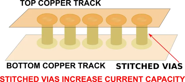
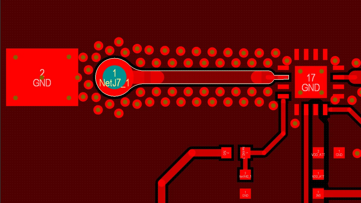
Via stitching refers to the placement of a periodic array of vias that connect copper planes, typically ground planes, across different layers in a multilayer PCB. These vias create a low-impedance path for high-frequency currents, ensuring continuity where planes might otherwise split or transition. In high-speed designs, discontinuities in reference planes can lead to increased loop inductance, which radiates energy as EMI. Via stitching addresses this by providing short return paths close to signal traces, minimizing field leakage.
The relevance of via stitching grows with the proliferation of high-speed interfaces like PCIe, USB4, and DDR5, where harmonics extend into GHz ranges. Poor ground plane integrity can cause crosstalk, ground bounce, and compliance failures during EMI testing. According to IPC-2221 guidelines for printed board design, maintaining robust interconnections between layers is essential for performance. This technique not only reduces EMI but also improves thermal management and power distribution. For electric engineers, mastering via stitching means achieving reliable designs that pass regulatory standards on the first iteration. For deeper insights into advanced via techniques, see our Ultimate Guide to Via Design in High-Tg PCBs.
Technical Principles of Via Stitching for EMI Reduction
At its core, via stitching works by reducing the inductance of current return paths in the PCB stackup. High-frequency signals seek the path of least impedance, and splits or gaps in planes force currents to detour, enlarging loop areas that act as antennas. An array of stitching vias shorts these gaps, confining electromagnetic fields between planes and preventing radiation. This creates a waveguide-like structure where fields propagate internally rather than escaping as EMI.
The effectiveness hinges on the spacing of the vias relative to the wavelength of the highest frequency component. A common guideline is to space vias at less than one-twentieth of the wavelength, known as the λ/20 rule, to ensure the structure blocks fields up to that frequency. For instance, denser arrays perform better at higher frequencies by approximating a continuous Faraday cage. In multilayer boards, stitching multiple ground planes together further lowers overall impedance, reducing common-mode noise. Simulations often reveal that stitched designs exhibit significantly lower radiated emissions compared to unstitched ones.
Shielding via stitching also controls crosstalk between adjacent traces. By placing vias along the edges of signal routing areas, engineers form a picket-fence barrier that attenuates coupled fields. This is particularly vital near layer transitions, where via stubs can otherwise resonate and amplify interference. The technique complements other PCB shielding techniques by integrating seamlessly into the layout without additional cost or board area.
Suggested Reading: The Ultimate Guide to Via Stitching in Multi Layer PCBs: Best Practices
Mechanisms Behind Via Stitching Effectiveness for EMI
The primary mechanism for EMI reduction via stitching lies in providing a dominant low-inductance return path for signal currents. In unstitched designs, return currents spread across discontinuous planes, creating large loops with high inductance that radiate efficiently. Stitching vias force currents through short, vertical paths, minimizing loop area and thus radiated power. This effect is frequency-dependent; at low frequencies, fewer vias suffice, but GHz signals demand tighter spacing.
Another key aspect is field confinement. Electromagnetic fields around a signal trace tend to expand if no nearby return path exists, coupling to nearby circuits or radiating outward. Stitching vias act as a coaxial shield, localizing fields within the via-signal-via triad and suppressing propagation. For differential pairs, arrays on both sides maintain balance and reduce common-mode conversion. In power planes, stitching prevents voltage droops that could modulate switching noise into EMI.
Limitations exist based on frequency and implementation. Beyond the cutoff where spacing equals λ/10 or λ/20, the structure becomes transparent to waves, reducing effectiveness. Drill wander or plating voids can also degrade performance, underscoring the need for manufacturing controls per IPC-A-600 acceptability criteria. Engineers must balance density with fabrication yields to optimize via stitching effectiveness for EMI.
Practical Solutions and Best Practices
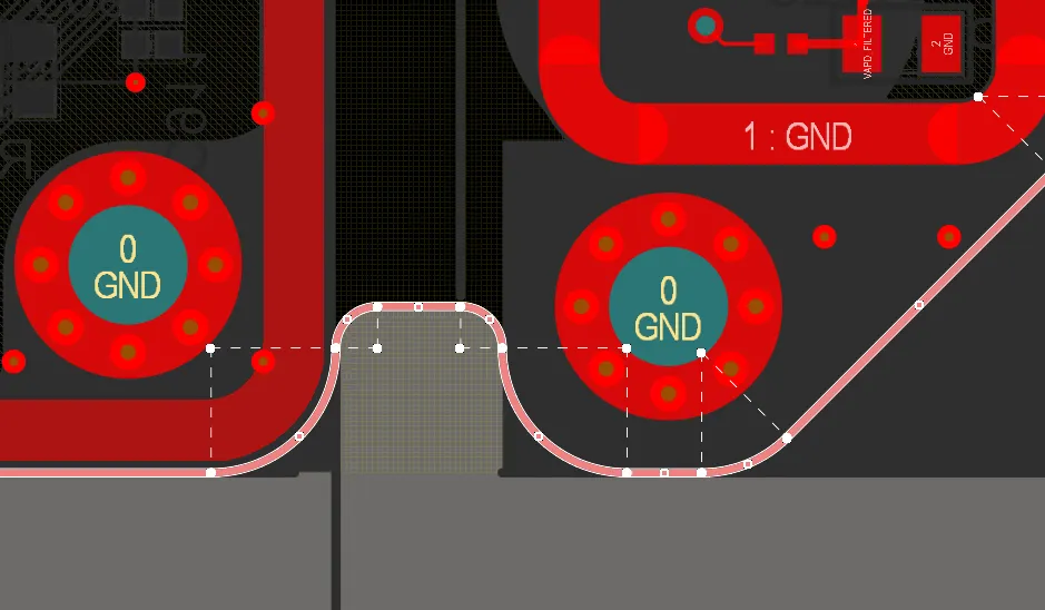
Implementing via stitching begins with identifying critical areas: plane splits, high-speed trace bends, and board edges. Place rows or grids of vias along these features, starting with a pitch of λ/20 calculated from the maximum harmonic frequency. For a 1 GHz signal, this equates to spacing around 15 mm in FR-4 (velocity factor adjusted), but tighter for margins. Connect all ground nets to avoid isolated islands.
Around sensitive analog sections, encircle with via fences to form shielded enclosures, enhancing isolation. For edge shielding, run a perimeter row every few millimeters to block slot antennas formed by board outlines. In power-ground pairs, stitch both planes to maintain decoupling capacitor effectiveness. Always verify with 3D field solvers during design to predict EMI performance.
Fabrication considerations include via size and protection. Use standard through-hole vias with adequate annular rings to prevent cracking under thermal stress, as specified in IPC-6012 performance standards. Avoid placing stitches directly under components or near high-current paths to prevent hotspots. Post-layout, run design rule checks for spacing and net continuity.
During prototyping, measure pre- and post-stitching emissions in a semi-anechoic chamber to quantify improvements. Common pitfalls include insufficient density or misalignment with signals, leading to hotspots of radiation. Automate placement where possible for consistency across large boards.
Advanced Applications and Troubleshooting
In RF and microwave designs, via stitching extends to microstrip-to-stripline transitions, where arrays suppress mode conversion. For mixed-signal boards, isolate digital and analog grounds with partial stitching, allowing DC separation while RF shorting. Troubleshooting high EMI often reveals unstitched plane gaps; adding vias post-simulation can resolve peaks.
Case insights from high-speed prototypes show that perimeter stitching alone cuts edge emissions by creating a continuous ground reference. Combine with guard traces for ultimate PCB shielding techniques. Monitor via reliability in harsh environments, ensuring plated-through integrity.
Conclusion
Via stitching stands out as an essential tool for EMI reduction via stitching in PCBs, offering engineers a cost-effective way to enhance shielding and signal integrity. By understanding its principles of low-inductance paths and field confinement, designers can implement targeted arrays that comply with EMC demands. Adhering to spacing rules like λ/20 and standards such as IPC-2221 ensures robust results. Integrate this technique early in the layout process for optimal via stitching effectiveness for EMI. Ultimately, it transforms potential interference sources into contained structures, enabling reliable high-performance boards.
FAQs
Q1: What is the optimal spacing for via stitching to achieve EMI reduction?
A1: For effective EMI reduction via stitching, space vias at less than λ/20 of the highest frequency wavelength, adjusting for the PCB material's dielectric constant. This prevents field leakage through the array. Tighter spacing, like λ/10, suits higher frequencies but increases via count. Verify with simulations to balance performance and manufacturability. This approach aligns with common PCB shielding techniques for compliance.
Q2: How does via stitching improve PCB shielding techniques compared to other methods?
A2: Via stitching provides integrated shielding by interconnecting planes, creating low-impedance barriers without external cans. It excels in containing internal fields and return currents, outperforming partial pours alone. Placement flexibility allows targeted protection around traces. While not a standalone solution for extreme cases, it complements ground floods effectively. Engineers value its simplicity and minimal impact on board space.
Q3: When should electric engineers prioritize via stitching for EMI control?
A3: Prioritize via stitching in designs exceeding 100 MHz, multilayer stackups with plane splits, or high-speed interfaces prone to harmonics. It shines near layer changes and edges where radiation peaks. If simulations show return path discontinuities, add stitches immediately. This ensures via stitching effectiveness for EMI without overdesigning. Avoid in low-frequency DC boards to prevent unnecessary complexity.
Q4: Can via stitching affect signal integrity negatively?
A4: Improper placement, like too close to high-speed lines, can introduce stubs or capacitance, but correct implementation enhances integrity via stable references. Maintain clearance per design rules and align with signals. Benefits outweigh risks in most cases, reducing crosstalk. Test iteratively for confirmation.
References
IPC-2221B — Generic Standard on Printed Board Design. IPC, 2012
IPC-A-600K — Acceptability of Printed Boards. IPC, 2020
IPC-6012E — Qualification and Performance Specification for Rigid Printed Boards. IPC, 2017