Introduction
AI accelerator PCBs play a critical role in modern automotive systems, powering advanced driver-assistance systems (ADAS) and autonomous driving features. These boards host high-performance processors that handle real-time data from sensors, cameras, and radar for tasks like object detection and path planning. In the harsh automotive environment, they must withstand extreme temperatures, vibrations, and electromagnetic interference while ensuring split-second reliability. Engineers designing AI accelerator PCB automotive solutions face unique challenges due to the integration of dense, power-hungry components on compact boards. This article explores how to meet stringent safety and reliability standards through proven engineering practices. By focusing on functional safety AI PCB principles, designers can deliver boards that support safer vehicles.
What Are AI Accelerator PCBs in Automotive Applications?
AI accelerator PCBs are specialized printed circuit boards optimized for edge computing in vehicles, featuring high-speed interconnects and thermal management for AI inference engines. They differ from standard PCBs by incorporating high-layer counts, often 12 to 20 layers, to support signal integrity at data rates exceeding 50 Gbps. In automotive contexts, the automotive PCB processes massive parallel computations for neural networks, requiring low-latency pathways between accelerators, memory, and interfaces like PCIe or Ethernet. The relevance stems from the shift toward software-defined vehicles, where AI drives features from adaptive cruise control to full self-driving. Reliability failures here could lead to catastrophic outcomes, making automotive PCB design guidelines essential from concept to production. Engineers must balance performance density with robustness against automotive stressors like thermal cycling and humidity.
Why Safety and Reliability Standards Matter for Functional Safety AI PCBs
Functional safety AI PCB design prioritizes preventing systematic and random failures in safety-critical systems. Automotive environments demand boards that operate flawlessly under -40°C to 125°C, constant vibration, and power fluctuations. Standards like ISO 26262 provide a framework for achieving Automotive Safety Integrity Levels (ASIL) from A to D, guiding hazard analysis and risk assessment for PCB-related elements. Compliance ensures that AI accelerators contribute to overall system safety without introducing single points of failure. For instance, ISO 26262 requires traceability of design decisions to safety goals, influencing everything from material selection to verification testing. Neglecting these elevates risks in ADAS, where millisecond delays can have severe consequences.
Key Standards Governing AI Accelerator PCB Automotive Development
ISO 26262 addresses functional safety across the development lifecycle, mandating processes for hardware like PCBs in AI systems. It emphasizes fault-tolerant architectures, such as redundant power rails and error-correcting codes on high-speed buses. For qualification, IPC-6012DS outlines performance specs for rigid boards in high-reliability automotive uses, specifying criteria for plating thickness, hole walls, and bow/warp limits. These standards ensure PCBs endure accelerated life testing simulating years of vehicle operation. JEDEC J-STD-020E further supports by classifying moisture sensitivity, critical for reflow soldering of AI components without delamination. Together, they form the backbone of ISO 26262 AI PCB compliance, enabling engineers to quantify and mitigate risks systematically.
Standards vs. PCB Requirements Table
| Standard | Key Focus | PCB Impact | ASIL Relevance |
|---|---|---|---|
| ISO 26262 | Functional safety lifecycle | Redundancy, diagnostics, FIT <10 for ASIL-D, traceability | All levels; ASIL-D demands highest diagnostic coverage |
| IPC-6012DS | High-reliability rigid boards | Plating thickness, bow/warp <0.75%, cleanliness, via reliability | Class 3/A for automotive safety-critical boards |
| AEC-Q104 / AEC-Q100 | Component & board qualification | Thermal cycling (1000+ cycles), HAST, vibration, SIR testing | Ensures materials and assembly survive automotive life |
| JEDEC J-STD-020E / IPC-TM-650 | Moisture sensitivity & insulation | MSL classification, baking protocols, CAF resistance | Prevents delamination and electrochemical migration in humid conditions |
| IATF 16949 | Automotive quality management | Traceability, process controls, supplier auditing | Mandatory for production of safety-critical AI accelerator PCBs |
These standards collectively ensure that functional safety AI PCB implementations achieve the required probabilistic metrics while remaining manufacturable at volume.
Automotive PCB Design Guidelines for High-Performance AI Accelerators
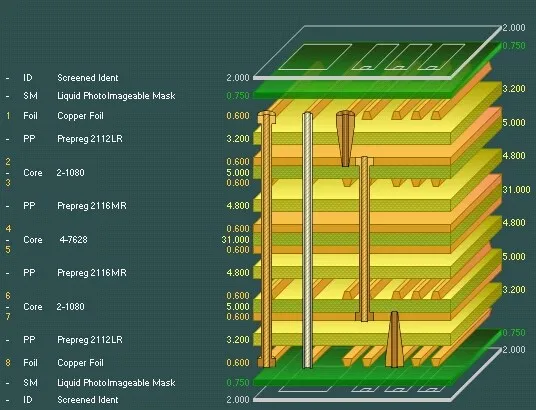
Effective automotive PCB design guidelines start with stack-up optimization to minimize crosstalk and maintain impedance control for SerDes lanes. Designers should allocate dedicated planes for power delivery to AI chips, using wide traces or embedded capacitors to handle transient currents up to hundreds of amps. Signal routing demands length-matched pairs and via-in-pad techniques to preserve eye diagrams at 112 Gbps PAM4 signaling. Thermal vias under hotspots, coupled with copper-filled vias, dissipate heat from accelerators exceeding 100W. Component placement prioritizes decoupling caps near power pins and shields for sensitive analog sections. These practices align with functional safety AI PCB needs, reducing electromagnetic emissions that could interfere with vehicle sensors. A symmetric multilayer configuration with dedicated reference planes is critical—see our guide on optimizing PCB stack-up for high-speed AI signals in automotive systems.
Layer sequencing influences both electrical and mechanical integrity. Ground planes adjacent to signal layers shield against noise, while core dielectrics with low loss tangents support high-frequency AI data paths. Engineers must model power distribution networks early to avoid voltage droops during peak inference loads. For AEC-Q100 AI PCB qualification, though primarily for ICs, the board design must accommodate graded components through robust solder joints and underfill. HDI structures with microvias enable denser integration, but require controlled impedance verification via TDR measurements. Adhering to these guidelines ensures the PCB supports AI accelerator PCB automotive demands without compromising safety.
Material Selection for Reliability in Harsh Environments
Material choices define the longevity of AI accelerator PCBs in automotive use. High-Tg laminates, typically above 170°C, resist delamination during soldering and operation. Low-CTE resins match coefficients with copper to prevent cracking under thermal stress. For functional safety AI PCB, halogen-free materials reduce toxicity risks in fires, while high-purity copper foils minimize electromigration in high-current paths. CAF-resistant formulations combat conductive anodic filamentation in humid conditions. Engineers evaluate these via bake tests and ionic contamination checks to predict field performance.
Here is a comparison of common materials for AI accelerator PCBs in automotive use:
| Material Type | Tg (°C) | CTE (ppm/°C) | Key Benefits | Typical Use Case |
|---|---|---|---|---|
| High-Tg FR-4 | 170–190 | 25–40 | Cost-effective, good thermal stability | General high-reliability layers |
| Polyimide | 250+ | 15–25 | Superior thermal & mechanical resilience | Extreme temperature zones |
| Low-loss Hydrocarbon | 200+ | Low | Excellent signal integrity at high speeds | High-frequency AI interconnects |
| CAF-Resistant Epoxy | 180+ | Controlled | Resistance to conductive anodic filamentation | Humid or high-voltage environments |
Thick copper, 2-3 oz, aids thermal spreading but demands adjusted etch factors for fine lines under 50μm. Sequential lamination builds complex stacks without stressing inner layers. For ISO 26262 AI PCB, material datasheets must include qualification data aligning with ASIL requirements. Hybrid stacks blending high-speed and RF dielectrics optimize AI signal chains. Surface finishes like ENIG or ENEPIG ensure wire bondability and corrosion resistance over 15-year lifespans.
Suggested Reading: AI Accelerator PCBs in Edge Computing: Design Considerations for Harsh Environments
Power Delivery and Signal Integrity Optimization
Robust power delivery uses multi-stage decoupling, plane stitching, and sometimes integrated voltage regulators to maintain stable supplies during dynamic AI workloads. Simulations of PDN impedance help identify and mitigate resonances.
Signal integrity optimization involves controlled impedance routing, minimal via stubs, and retimers or equalizers for longer channels. Differential pairs with tight skew control and shielding guard traces reduce crosstalk and EMI. Early 3D electromagnetic simulations and TDR measurements validate performance, ensuring low-latency, error-free data paths essential for real-time AI inference in vehicles.
Manufacturing and Assembly Best Practices
Manufacturing AI accelerator PCB automotive boards requires precision to meet IPC-6012DS tolerances, such as annular ring minimums of 50μm. Laser direct imaging for photoplotting achieves sub-25μm features for HDI. Controlled impedance panels undergo flying probe testing before build. Solder mask registration tighter than 75μm prevents bridging on fine-pitch BGAs for AI chips. Baking removes moisture per JEDEC J-STD-020E classifications, avoiding popcorn effects in reflow.
Assembly focuses on warpage control below 0.75% for large panels, using carriers for thin cores. Nitrogen reflow profiles minimize oxidation on power devices. X-ray inspection verifies BGA voids under 25%, crucial for AEC-Q100 AI PCB thermal cycling endurance. Conformal coatings protect against salt spray and fluids. Traceability via lot coding supports ISO 26262 fault tree analysis. These steps yield boards ready for system-level qualification.
Testing and Qualification Strategies
Reliability testing simulates automotive lifetimes through temperature cycling (-55°C to 125°C, 1000 cycles), vibration (10-2000 Hz), and power cycling. SIR testing per IPC-TM-650 verifies insulation resistance post-HAST. Cross-section analysis confirms via integrity after stress. For functional safety AI PCB, FMEDA calculates failure rates below 10 FIT for ASIL-D. Burn-in screens early failures in accelerators. These validate automotive PCB design guidelines in practice.
Real-World Case Studies and Lessons from ADAS Deployments
In production ADAS systems, one OEM addressed thermal hotspots in AI accelerators by implementing copper-filled thermal vias and hybrid high-Tg materials, significantly reducing junction temperatures and improving MTBF. Another deployment used redundant power domains and HDI microvias to achieve ASIL D compliance for emergency braking, eliminating single-point failures identified in early FMEDA.
Lessons learned include the importance of early PDN and signal integrity simulations to avoid costly respins, and the value of supplier collaboration under IATF 16949 for consistent material quality. Overlooking warpage control during assembly led to yield issues in one case, highlighting the need for tight process windows in high-layer boards.
Challenges in AI Accelerator PCB Automotive Design and Solutions
High power density causes hotspots, addressed by vapor chambers or embedded heat pipes. Signal integrity degrades with length, mitigated by retimers or equalizers. Supply chain variability demands qualified suppliers with IATF 16949 processes. Cost pressures favor optimized via farms over blind/buried excess. Engineers use DFMEA to prioritize mitigations aligning with ISO 26262.
2026 Trends in Automotive AI PCB Technology
In 2026, trends include wider adoption of ultra-high-layer HDI with advanced microvia stacking, integration of AI-specific packaging (e.g., 2.5D/3D with high-bandwidth memory), and hybrid materials for better thermal-electrical performance. Edge AI accelerators are becoming more power-efficient while supporting higher inference rates.
Increased focus on functional safety drives redundant architectures and AI-specific diagnostics. Sustainability pushes halogen-free and recyclable materials. The rise of software-defined vehicles encourages modular PCB designs that support over-the-air updates and future scalability, with automotive AI PCB technology playing a central role in enabling Level 3+ autonomy.
Conclusion
AI accelerator PCBs for automotive applications demand meticulous attention to safety and reliability to enable next-generation mobility. By integrating ISO 26262 principles, IPC-6012DS specs, and robust design guidelines, engineers create boards that excel in extreme conditions. Key takeaways include thermal-aware layouts, qualified materials, and rigorous testing. These ensure functional safety AI PCB performance, paving the way for trustworthy ADAS. Automotive stakeholders benefit from standardized approaches that reduce risks and accelerate deployment.
FAQs
Q1: What role does ISO 26262 play in AI accelerator PCB automotive design?
A1: ISO 26262 provides a comprehensive framework for functional safety AI PCB development, covering hazard analysis, design verification, and confirmation measures. It assigns ASIL levels to guide PCB fault tolerance, such as redundancy in power and signals. Compliance involves tools like FMEDA to quantify hardware metrics. This ensures AI systems mitigate risks in safety-critical functions like autonomous braking.
Q2: How do automotive PCB design guidelines address thermal management for AEC-Q100 AI PCB?
A2: Automotive PCB design guidelines emphasize via thermal resistance below 1°C/W and plane stitching for heat spreading. Thick copper pours and thermal pads under AI chips dissipate over 50W hotspots. Modeling with CFD predicts profiles during peak loads. These practices support AEC-Q100 qualified components by maintaining junction temperatures under limits, enhancing reliability in engine bays.
Q3: What are essential tests for functional safety AI PCB qualification?
A3: Key tests include thermal shock, vibration per ISO 16750, and HAST for humidity robustness. IPC-TM-650 methods assess solder joint integrity post-stress. Electrical tests verify continuity and isolation at elevated temps. These align with automotive PCB design guidelines, confirming zero failures over qualified cycles for ASIL compliance.
Q4: Why is IPC-6012DS critical for AI accelerator PCB automotive manufacturing?
A4: IPC-6012DS specifies stringent criteria for plating uniformity, hole quality, and cleanliness in high-reliability boards. It mandates bow/warp under 0.75% and conductor spacing for high voltage. This standard ensures PCBs withstand automotive stresses, supporting dense AI layouts without defects. Manufacturers use it for process controls and acceptance.
References
ISO 26262 — Road vehicles – Functional safety. ISO, 2018
IPC-6012DS — Qualification and Performance Specification for Rigid Printed Boards for High Reliability Automotive Applications. IPC, 2016
JEDEC J-STD-020E — Moisture/Reflow Sensitivity Classification for Nonhermetic Surface Mount Devices. JEDEC, 2014


