Introduction
Flexible printed circuit boards expand design possibilities in compact, high-mobility electronics like wearables, medical devices, and automotive sensors. The flexible PCB assembly process requires precision to handle material flexibility without compromising reliability. Engineers face unique hurdles such as substrate deformation, trace cracking during bending, and solder joint stress in dynamic environments. This article delves into the flexible PCB assembly process, flexible PCB soldering techniques, flexible PCB component placement, and flexible PCB testing. By focusing on practical strategies, professionals can minimize failures and enhance product lifespan. Reliability starts with understanding how assembly choices impact performance under repeated flexing.
Understanding Flexible PCB Assembly
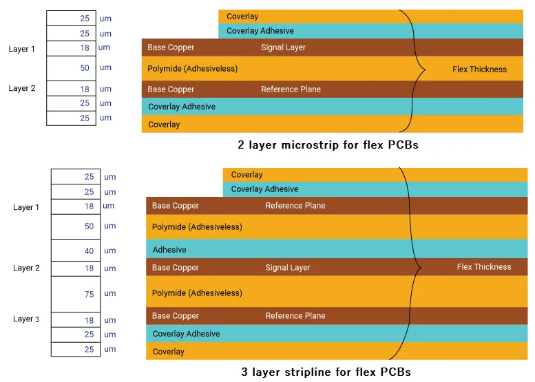
Flexible PCB assembly involves mounting components onto thin, bendable substrates typically made from polyimide or polyester films. The process adapts surface-mount technology (SMT) and through-hole methods to accommodate the board’s pliability, often using carrier fixtures for stability. Key stages include stencil printing, component placement, reflow soldering, and post-assembly inspection. Unlike rigid boards, flex circuits demand controlled handling to prevent creasing or tearing during transport between stations. Engineers must consider bend radius limitations early to avoid stress concentrations that lead to fatigue over time. Adhering to qualification standards like IPC-6013D ensures the assembly meets performance criteria for flex and rigid-flex constructions.
The assembly workflow begins with solder paste application through laser-cut stencils optimized for thin traces. Components then undergo precise pick-and-place operations, followed by thermal profiling in reflow ovens. Cleaning removes flux residues that could cause ionic contamination in tight spaces. Final shaping, such as singulation from panels, requires gentle tools to preserve integrity. Troubleshooting early defects, like paste bridging, prevents yield losses downstream.
This issue is one example within the broader context of Flexible PCBs: Materials, Fabrication, and Applications.
Flexible PCB Soldering Techniques
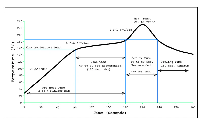
Flexible PCB soldering techniques prioritize low thermal stress to protect delicate substrates and traces. Reflow soldering dominates due to its uniformity, but profiles must ramp slowly to avoid warping polyimide layers. Preheating stabilizes the assembly, while peak temperatures stay below 260 degrees Celsius for most materials. Hand soldering suits prototypes or repairs, using fine-tip irons with temperature control under 350 degrees Celsius. Wave soldering applies selectively for through-hole parts, with flux tailored for flex surfaces to minimize voids.
J-STD-001H outlines requirements for soldered assemblies, emphasizing criteria for flexible boards like fillet formation and hole fill. Engineers troubleshoot common issues by analyzing X-ray images for hidden voids or inspecting under magnification for cold joints. Vapor phase soldering offers an alternative for uniform heating in high-density designs, reducing oxidation risks. Post-solder baking removes moisture trapped during processing, enhancing joint longevity. Selecting lead-free alloys compatible with flex materials prevents embrittlement during cycles.
Vapor phase excels in prototypes where convection ovens might unevenly heat curved sections. Always validate profiles with thermocouples placed at critical points like stiffeners or fold areas. Flux choice impacts cleanliness; no-clean types reduce residues but demand verification for electrical performance.
Flexible PCB Component Placement
Flexible PCB component placement demands strategic positioning to distribute mechanical stress evenly across bend zones. Components in dynamic flex regions risk cracking under repeated cycles, so engineers prefer passive parts or low-profile SMDs there. Rigid sections or stiffeners host active devices like ICs for stability during handling and testing. Fiducials ensure alignment accuracy within 50 microns, compensating for substrate stretch. Carrier panels support the flex during pick-and-place, preventing distortion from vacuum nozzles.
Placement rules follow design guidelines that limit density near bend lines, typically spacing components 0.5 mm from flex tails. High-mass parts like connectors anchor in rigid-flex transitions to avoid tearing. Software simulates strain, guiding layout revisions pre-assembly. Troubleshooting misalignment involves adjusting machine vision for substrate transparency effects. Post-placement verification uses automated optical inspection (AOI) to flag offsets early.
Orienting polarized components parallel to bend axes reduces shear forces. For multilayer flex, align vias away from fold lines to prevent microcracks. Iterative testing refines placement for specific applications like folding displays.
Flexible PCB Testing Protocols
Flexible PCB testing verifies electrical continuity, mechanical endurance, and environmental resilience post-assembly. In-circuit testing (ICT) probes nets while the board lies flat on carriers, avoiding direct flex pressure. Flying probe suits low-volume runs for its flexibility in accessing fine-pitch pads. Functional testing simulates end-use conditions, including powered bending cycles. IPC-A-610H defines acceptability criteria for solder joints and component alignment on flex assemblies.
Mechanical tests like cyclic bending assess fatigue life, using mandrels sized to minimum bend radii. Thermal shock screens for delamination by cycling between extremes. Ionic contamination testing measures residues that accelerate corrosion in humid environments. X-ray and cross-section analysis detect subsurface defects like trace breaks. Data logging tracks resistance changes over thousands of cycles.
Environmental chambers combine humidity, vibration, and temperature to mimic real-world stress. Burn-in accelerates aging, revealing early failures. Comprehensive protocols correlate lab results with field reliability.
Best Practices for Reliable Assembly
Integrate design-for-assembly (DFA) early by specifying bend allowances and stiffener locations. Use polyimide coverlays for trace protection during handling. Automated lines with soft grippers minimize creases. Bake boards pre-assembly to expel moisture below 0.1 percent weight gain. Profile ovens with nitrogen atmospheres cut oxidation in fine-pitch soldering.
Validate processes via statistical process control (SPC), monitoring paste volume and placement accuracy. Train operators on flex-specific handling to avoid fingerprints or folds. Collaborate between design and assembly teams for iterative improvements. Document deviations with root-cause analysis for continuous refinement.
For more knowledge about Flexible PCB Assembly, see our comprehensive guide: Flexible PCB Assembly Techniques: A Comprehensive Guide
Troubleshooting Common Assembly Issues
Warpage during reflow often stems from asymmetric copper distribution; balance layers or add constraining fixtures. Solder beading on flex tails results from gravity in vertical ovens, solved by horizontal profiling. Trace cracking in bend zones indicates excessive radius violation; redesign or reinforce with adhesive. Component tombstoning links to rapid paste drying, addressed by optimized stencil apertures. Delamination post-testing points to poor adhesion; verify coverlay lamination per specs.
Electrical opens after flexing suggest microcracks; perform dye-and-penetrant analysis. Yield drops from handling damage call for vacuum-formed carriers. Systematic logging isolates variables like humidity spikes.
Conclusion
Mastering flexible PCB assembly hinges on tailored processes for soldering, placement, and testing that prioritize material limits. Engineers achieve reliability by integrating standards-guided practices with hands-on troubleshooting. Key takeaways include slow thermal ramps, strategic component siting, and exhaustive bend cycling. These methods extend service life in demanding applications. Forward-thinking assembly elevates flexible PCBs from innovative to indispensable.
FAQs
Q1: What are the main steps in the flexible PCB assembly process?
A1: The flexible PCB assembly process starts with solder paste printing on carrier-supported flex circuits, followed by precise component placement using vision systems. Reflow soldering applies controlled profiles to form joints without substrate damage. Cleaning and inspection precede shaping and functional testing. This sequence ensures alignment with reliability standards, minimizing defects like voids or misalignment. Carriers prevent distortion throughout.
Q2: How do flexible PCB soldering techniques differ from rigid boards?
A2: Flexible PCB soldering techniques use slower reflow ramps and lower peaks to avoid warping thin substrates, unlike rigid boards that tolerate higher stresses. J-STD-001H guides fillet quality and flux use for flex. Hand soldering employs fine tips for repairs, while vapor phase ensures uniformity. Nitrogen atmospheres reduce oxidation on exposed traces. These adaptations prevent cracking in dynamic areas.
Q3: What challenges arise in flexible PCB component placement?
A3: Flexible PCB component placement challenges include substrate stretch affecting alignment and stress concentration in bend zones causing failures. Low-profile parts suit flex regions, while stiffeners support heavy components. Fiducials compensate for material movement during pick-and-place. Carriers stabilize thin boards, and simulations predict strain. Proper spacing from fold lines enhances cycle life.
Q4: Why is flexible PCB testing critical for reliability?
A4: Flexible PCB testing confirms endurance under bending, thermal cycling, and vibration, revealing issues like trace fatigue early. Protocols include ICT, AOI, and cyclic flexing per IPC criteria. Environmental chambers simulate field conditions. Comprehensive testing correlates assembly quality with long-term performance, preventing field failures in mobiles or sensors.
References
IPC-6013D — Qualification and Performance Specification for Flexible Printed Boards. IPC, 2017
J-STD-001H — Requirements for Soldered Electrical and Electronic Assemblies. IPC, 2020
IPC-A-610H — Acceptability of Electronic Assemblies. IPC, 2018


