Introduction
In the realm of PCB manufacturing, ensuring electrical integrity stands as a cornerstone of quality control. Flying probe testing emerges as a pivotal method, offering unparalleled flexibility for diagnosing potential faults without the need for custom fixtures. This approach proves especially valuable in scenarios involving PCB prototype testing and low volume PCB testing, where traditional methods fall short due to time and cost constraints. Electric engineers appreciate its ability to adapt to diverse board designs, from simple single-layer to complex multilayer configurations. By automating probe movements across test points, it verifies continuity, detects shorts, and measures key parameters efficiently. As production demands evolve toward smaller batches and rapid iterations, flying probe testing positions itself as a reliable bed of nails alternative.
What Is Flying Probe Testing and Why It Matters
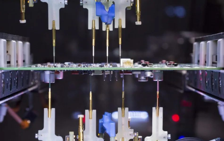
Flying probe testing involves a system where independent probes, typically mounted on robotic arms, move dynamically across the surface of a printed circuit board to make electrical contact at designated test points. Unlike fixture-based systems, this fixtureless testing eliminates the upfront investment in bespoke tooling, making it ideal for high-mix, low-volume production runs. Engineers rely on it to confirm netlist accuracy, identify opens, shorts, and incorrect connections before assembly proceeds. Its relevance intensifies in PCB prototype testing, where design changes occur frequently, rendering fixed fixtures obsolete quickly. Factory insights reveal that this method reduces turnaround times significantly, aligning with the need for agile manufacturing processes. Ultimately, it safeguards against downstream failures, enhancing overall yield and reliability in the production pipeline.
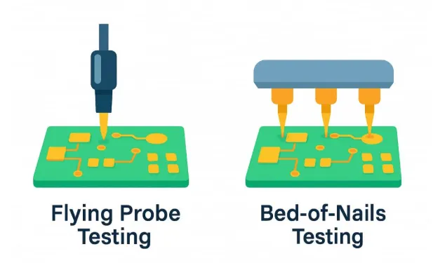
The distinction from bed of nails testing underscores its strategic importance. Bed of nails employs a rigid fixture with hundreds of spring-loaded pins that contact all points simultaneously for parallel testing, suited to high-volume runs. Flying probe, by contrast, sequences tests point-by-point, trading speed for versatility. This makes it a preferred PCB testing solution when board sizes vary or geometries challenge fixture design. In quality control environments, adopting flying probe testing minimizes risks associated with mechanical wear on fixtures and supports compliance with rigorous industry benchmarks.
Suggested Reading: The ROI of Flying Probe Testing: Justifying the Investment in PCB Quality
Technical Principles of Flying Probe Testing
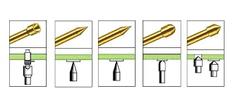
At its core, flying probe testing operates on principles of precise electromechanical positioning and electrical measurement. Probes, often four to eight in number with counterparts on both board sides, navigate via linear motors or servo systems guided by CAD-derived test programs. Each probe tip, engineered for minimal inductance and capacitance, contacts pads or vias to perform measurements such as resistance for continuity, isolation voltage for shorts, and sometimes capacitance for layer integrity. The system software compares results against golden board data or netlist specifications, flagging deviations in real-time. This sequential access allows testing of densely packed boards where fixture pins would interfere.
Key mechanisms include vector-based probe paths optimized to avoid collisions and reduce cycle times. Advanced systems incorporate vision cameras for fiducial alignment, ensuring sub-micron accuracy despite board warpage or tolerances. Electrical tests adhere to guidelines outlined in IPC-9252B, which specifies parameters like test voltage, current limits, and dwell times to prevent damage while maximizing fault detection. For instance, continuity tests apply low-voltage signals to verify paths below specified thresholds, while isolation ramps up to detect latent defects. These principles enable comprehensive coverage, often achieving over 90% of nets without physical constraints.
Multilayer boards benefit from through-hole and blind via probing, where probes access inner layers indirectly via capacitance mapping. Factory-driven calibration routines maintain probe cleanliness and force consistency, critical for reliable data. Integration with boundary scan or functional tests extends its utility into assembled boards, though bare board applications dominate.
Flying Probe as a Bed of Nails Alternative
Comparing flying probe testing to bed of nails highlights its role as a fixtureless testing powerhouse. Bed of nails excels in parallel execution, contacting all points at once for throughput in mass production, but demands precise fixture fabrication matching board revisions exactly. Any design tweak necessitates costly redesigns, impractical for PCB prototype testing. Flying probe sidesteps this by programming paths from Gerber files, adapting instantly to changes. While slower per board, its per-unit economics shine for low volume PCB testing, often costing a fraction of fixture development. For higher volumes where speed becomes critical, see our guide on ICT testing and bed-of-nails fixtures for high-volume PCB assembly.
Practical trade-offs include test coverage and speed. Flying probe typically tests 80 to 100% of nets sequentially, sufficient for most diagnostics, whereas bed of nails achieves full parallelism but risks fixture-related artifacts like pin bending. In high-density interconnects, probe access surpasses fixed pins, probing finer pitches. Engineers select based on volume: under 100 boards favor flying probe for flexibility.
Practical Solutions and Best Practices for Implementation
Implementing flying probe testing requires strategic test point placement during design. Allocate 10 to 20% of nets with accessible pads, prioritizing high-risk nets like power and ground planes. Avoid placing points under components or in tight arrays to ensure probe reach. Software optimization merges common paths, minimizing travel distance and boosting efficiency. Pre-test simulations validate coverage, identifying unreachable nodes early.
Best practices emphasize netlist import accuracy and golden board establishment. Generate test programs from ODB++ or IPC-D-356 formats for fidelity. Calibrate probes daily, using IPC-A-600K criteria for visual acceptability before electrical runs. Combine with automated optical inspection for hybrid fault detection. For low volume PCB testing, batch similar boards to amortize setup.
Troubleshooting common issues involves analyzing false calls from contamination or misalignment. Clean boards ultrasonically and use contact force monitoring to mitigate. If capacitance tests fail on multilayers, verify stackup data. These steps ensure robust diagnostics aligned with performance specs in IPC-6012E.
In production, integrate flying probe early post-fabrication, before routing or scoring. Monitor metrics like first-pass yield and escape rates to refine processes. For PCB prototype testing, iterate tests with engineering changes swiftly.
Insights from Factory Applications
Factory experiences underscore flying probe's prowess in diverse scenarios. During transitions from prototype to pilot runs, it bridges gaps left by evolving designs. One insight reveals its efficacy in detecting drill breakout or plating voids missed by visual checks. Engineers leverage parametric tests for resistance profiling across traces, correlating to IPC standards.
In high-mix environments, quick reprogramming handles variants without downtime. Pairing with X-ray for inner layer verification enhances confidence. These applications affirm its status as a versatile PCB testing staple.
Conclusion
Flying probe testing revolutionizes PCB diagnostics through its fixtureless, adaptable nature, excelling as a bed of nails alternative for PCB prototype testing and low volume PCB testing. Its technical precision, from probe navigation to electrical measurements, ensures fault detection per industry guidelines. Practical adoption demands thoughtful design and calibration, yielding high reliability. Electric engineers benefit from its cost-efficiency and speed in dynamic production. Embracing this method fortifies quality control, minimizing risks in complex assemblies.
FAQs
Q1: What is flying probe testing in PCB manufacturing?
A1: Flying probe testing is a fixtureless PCB testing method using movable robotic probes to check electrical continuity, shorts, and resistance at test points. It suits low volume PCB testing by eliminating custom fixtures, enabling rapid programming from design files. Compliance with IPC-9252B ensures accurate parameters like voltage and dwell time. This approach detects opens and misroutes effectively, supporting prototype iterations without delays. Factories value its versatility for high-mix runs.
Q2: How does flying probe testing serve as a bed of nails alternative?
A2: Flying probe testing replaces bed of nails by sequentially accessing points with dynamic probes, avoiding fixture costs and redesigns. Ideal for PCB prototype testing, it handles design changes instantly via software updates. While slower for high volumes, it offers superior access to fine-pitch pads. Coverage matches most needs, per IPC-6012E specs. Engineers prefer it for flexibility in quality control.
Q3: When is flying probe testing best for low volume PCB testing?
A3: Opt for flying probe in low volume PCB testing under 500 boards, prototypes, or frequent revisions where fixtures prove uneconomical. It verifies netlists comprehensively without tooling lead times. Best practices include ample test points and netlist validation. It excels in detecting subtle faults like high-resistance joints. This method aligns factory workflows for agile production.
Q4: Can flying probe testing handle assembled PCBs?
A4: Yes, flying probe testing extends to assembled PCBs for in-circuit checks, though bare boards dominate. Probes navigate around components to test nodes, measuring passive values. Vision alignment aids precision. It complements functional tests in low volume scenarios. Adhere to IPC-A-600K for board acceptability pre-test.
References
IPC-9252B — Requirements for Electrical Testing of Unpopulated Printed Boards. IPC, 2016
IPC-6012E — Qualification and Performance Specification for Rigid Printed Boards. IPC, 2017
IPC-A-600K — Acceptability of Printed Boards. IPC, 2020


