Introduction
High-Density Interconnect (HDI) PCBs have emerged as a pivotal technology in modern electronics, enabling compact and high-performance designs. In the realm of construction equipment, where reliability and durability are paramount, integrating HDI PCB construction equipment solutions can offer significant advantages. These boards, characterized by microvias, blind vias, and buried vias, allow for denser component placement and improved signal integrity. However, their adoption in heavy-duty applications like construction machinery raises questions about cost, complexity, and environmental resilience. This article explores the technical aspects of HDI PCBs, focusing on their relevance to construction equipment. It examines the benefits and challenges of using microvias and laser drilling HDI techniques in such demanding environments. The goal is to provide electrical engineers with a clear understanding of whether this technology aligns with their project needs.
What Are HDI PCBs and Why Do They Matter in Construction Equipment?
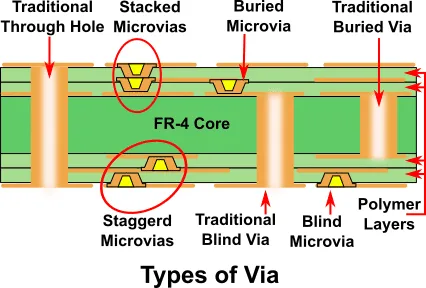
HDI PCBs are advanced printed circuit boards designed to accommodate a higher number of components in a smaller footprint. They achieve this through finer traces, smaller vias, and multiple layers interconnected by microvias, blind vias, and buried vias. Unlike traditional PCBs, HDI boards use laser drilling HDI methods to create precise, small-diameter vias, enabling complex routing in limited space. This technology is widely recognized under standards like IPC-2226, which outlines design guidelines for high-density interconnect structures. For a deeper look at these via structures, see our guide to microvias in HDI PCBs.
In construction equipment, electronic systems control critical functions such as engine management, hydraulic systems, and operator interfaces. The harsh operating conditions, including vibration, dust, and temperature extremes, demand robust and reliable electronics. HDI PCBs matter here because they support miniaturization without sacrificing performance. They allow for integration of advanced features like real-time diagnostics and telematics in compact control units. However, their implementation must balance technical benefits against practical challenges specific to this industry.
Technical Principles of HDI PCBs in Construction Equipment
Core Features of HDI Technology
HDI PCBs rely on several key elements to achieve high density. Microvias, typically less than 0.15 mm in diameter, are created using laser drilling HDI processes. These small vias connect adjacent layers, reducing signal path length and enhancing electrical performance. Blind vias connect an outer layer to an inner layer without passing through the entire board, while buried vias link internal layers only, remaining invisible on the surface. Both types, as defined in IPC-6012E, optimize space and improve routing efficiency.
The use of thinner dielectric materials and finer line widths, often below 0.1 mm, further contributes to density. These characteristics allow HDI PCBs to support high-speed signals with reduced interference, a critical factor for data-intensive systems in modern construction machinery.
Application in Harsh Environments
Construction equipment operates in environments that test the limits of electronic components. HDI PCBs must withstand mechanical stress, thermal cycling, and exposure to contaminants. Their multilayer structure can enhance durability by distributing stress across layers, but the small size of microvias and intricate designs may pose reliability risks if not manufactured to strict standards like IPC-A-600K. Signal integrity also benefits from shorter interconnects, reducing latency in systems that monitor equipment status or control automated functions.
Manufacturing Techniques
Laser drilling HDI technology is central to creating microvias with precision. This method ensures accurate hole placement and minimal damage to surrounding materials, adhering to guidelines in IPC-2226 for via formation. Sequential lamination processes are often used to build multilayer HDI boards, embedding blind and buried vias during fabrication. These techniques increase complexity but are essential for achieving the density required in compact control modules for construction equipment. Engineers often combine this with sequential lamination techniques for optimal results.
HDI vs Standard PCBs in Construction Equipment: Side-by-Side Comparison
| Aspect | Standard PCBs | HDI PCBs | Advantage in Construction Equipment |
|---|---|---|---|
| Component Density | Lower (larger traces, through-hole vias) | Significantly higher (microvias, fine lines) | Enables compact control units in space-constrained machinery |
| Board Size & Weight | Larger and heavier | 30–50% smaller and lighter | Reduces overall equipment weight; improves fuel efficiency and handling |
| Via Technology | Mechanical through-holes | Laser-drilled microvias, blind/buried vias | Shorter signal paths; better routing in tight spaces |
| Signal Integrity | Adequate for basic applications | Superior (reduced parasitics, up to 2.5× faster signals) | Critical for real-time sensors and telematics |
| Layer Count | Higher for equivalent functionality | Fewer layers possible | Simplifies assembly; lowers long-term costs |
| Reliability in Harsh Conditions | Good but bulkier design | Enhanced when properly plated/filled | Better vibration and thermal resistance |
| Cost (per board) | Lower upfront | 20–50% higher | Offset by system-level savings (see ROI section) |
Benefits of HDI PCBs in Construction Equipment
Compact Design for Space Constraints
Construction equipment often has limited space for electronic assemblies. HDI PCBs address this by enabling smaller, lighter control units. The use of microvias, blind vias, and buried vias allows engineers to pack more functionality into confined areas, such as dashboards or engine compartments. This compactness supports the integration of advanced features without increasing the physical size of the equipment.
Enhanced Signal Performance
Modern construction machinery increasingly relies on high-speed data for real-time monitoring and communication. HDI PCBs, with their shorter signal paths and reduced parasitic effects, improve signal integrity. This is vital for systems handling sensor data or wireless connectivity, ensuring accurate operation under dynamic conditions.
Improved Reliability with Proper Design
When designed and manufactured according to standards like IPC-6012E, HDI PCBs can offer high reliability. Their multilayer construction can protect critical connections from environmental stressors. Properly implemented blind vias and buried vias reduce the risk of external damage, making these boards suitable for rugged applications.
Challenges of Implementing HDI PCBs in Construction Equipment
Higher Manufacturing Costs
The advanced techniques required for HDI PCB construction equipment applications, such as laser drilling HDI and sequential lamination, lead to increased production costs. Creating microvias and ensuring precise alignment of blind and buried vias demands specialized equipment and expertise. For projects with tight budgets, this cost factor can be a significant barrier.
Design and Testing Complexity
Designing HDI PCBs requires careful planning to meet aspect ratio limits and via depth specifications as outlined in IPC-2226. Engineers must account for thermal expansion, mechanical stress, and signal routing in dense layouts. Testing these boards for reliability in harsh conditions adds another layer of complexity, often requiring extensive simulation and prototyping.
Environmental Durability Concerns
While HDI PCBs can be reliable, their fine features may be more susceptible to failure under extreme conditions. Microvias, if not properly plated or filled, can develop cracks or voids, leading to connectivity issues. Standards like IPC-A-600K emphasize the importance of inspection to detect such defects, but ensuring long-term durability in construction environments remains a challenge.
Best Practices for Using HDI PCBs in Construction Equipment
Adherence to Industry Standards
Compliance with recognized standards is non-negotiable. IPC-6012E provides specifications for qualification and performance of rigid HDI boards, while IPC-A-600K sets acceptability criteria for manufactured boards. Following IPC-2226 ensures proper design of high-density interconnects, including via structures and trace widths. These guidelines help mitigate risks associated with complex designs.
Robust Material Selection
Choosing materials with high thermal stability and mechanical strength is crucial for construction equipment applications. Dielectric materials should withstand temperature fluctuations and resist moisture absorption. Consulting material properties as per IPC standards can guide engineers in selecting appropriate substrates for HDI PCBs.
Thorough Testing Protocols
Before deployment, HDI PCBs must undergo rigorous testing for environmental stress, vibration, and thermal cycling. Accelerated life testing can simulate years of operation in harsh conditions, identifying potential failure points in microvias or buried vias. Adhering to testing protocols ensures the boards meet operational demands.
Collaboration with Fabrication Experts
Close coordination with fabrication teams during the design phase helps address manufacturability concerns. Engineers should specify requirements for laser drilling HDI processes and via filling techniques to avoid defects. Early collaboration ensures that design intent aligns with production capabilities, reducing the likelihood of costly revisions.
Real-World Case Studies & Future Trends
In modern excavators and cranes, HDI PCBs enable compact modules that integrate GPS, hydraulic sensors, and wireless communication in spaces smaller than a smartphone. One construction OEM reduced control-unit weight from 500 g to 300 g while adding real-time diagnostics—improving fuel efficiency and operator ergonomics. Similar deployments in bulldozers and loaders have demonstrated reliable performance under continuous vibration, with HDI designs cutting failure rates in sensor networks.
Looking ahead, HDI PCBs will power Industry 4.0 transformations in construction. Integration with IoT sensors, 5G telematics, and AI-driven predictive maintenance will demand even higher density and signal integrity. Ultra-HDI advancements (finer traces under 50 µm) and flexible-rigid hybrids will support autonomous machinery and drone-based site monitoring. Market projections show strong growth through 2032, driven by 5G infrastructure, smart equipment fleets, and sustainability-focused lightweight designs.
Conclusion
HDI PCBs offer compelling advantages for construction equipment, including compact design, enhanced signal performance, and potential reliability improvements. The use of microvias, blind vias, buried vias, and laser drilling HDI techniques enables sophisticated electronics in space-constrained, harsh environments. However, challenges such as higher costs, design complexity, and durability concerns must be carefully managed. By adhering to industry standards like IPC-6012E and IPC-2226, selecting robust materials, and implementing thorough testing, engineers can maximize the benefits of HDI PCB construction equipment applications. The decision to adopt this technology hinges on balancing project requirements with practical constraints, ensuring that performance gains justify the investment.
FAQs
Q1: What are the main advantages of using HDI PCB construction equipment solutions?
A1: HDI PCBs provide compact designs ideal for space-limited construction equipment. They support denser component placement using microvias, blind vias, and buried vias. This allows integration of advanced features like diagnostics in small control units. Additionally, shorter signal paths enhance performance for high-speed data systems, ensuring reliable operation under demanding conditions.
Q2: How does laser drilling HDI impact the production of PCBs for construction machinery?
A2: Laser drilling HDI enables precise creation of microvias, essential for high-density designs in construction machinery PCBs. This technique ensures accurate small-diameter holes, improving routing efficiency. However, it increases manufacturing complexity and cost, requiring specialized equipment. Proper execution, aligned with industry standards, is critical to avoid defects in harsh environments.
Q3: What challenges arise with blind vias and buried vias in rugged applications?
A3: Blind vias and buried vias optimize space in HDI PCBs but pose challenges in rugged applications like construction equipment. Their small size can lead to reliability issues if not properly manufactured. Defects in plating or filling may cause failures under vibration or thermal stress. Strict adherence to standards ensures durability in such conditions.
Q4: How can engineers ensure reliability of microvias in HDI PCBs for heavy equipment?
A4: Engineers can ensure microvia reliability in HDI PCBs for heavy equipment by following design guidelines in recognized standards. Thorough testing for environmental stress and vibration is essential. Selecting robust materials and coordinating with fabrication teams to perfect via formation processes also minimizes risks of cracks or connectivity issues.
References
IPC-6012E — Qualification and Performance Specification for Rigid Printed Boards. IPC, 2020.
IPC-A-600K — Acceptability of Printed Boards. IPC, 2020.
IPC-2226 — Sectional Design Standard for High Density Interconnect (HDI) Printed Boards. IPC, 2017.


