Introduction
Military communication systems rely on printed circuit boards (PCBs) to transmit vast amounts of data at high speeds, often in demanding environments. High-speed PCB design becomes critical to maintain reliable performance under these conditions. Signal integrity ensures that digital signals arrive at their destination with minimal distortion, preventing data errors that could compromise mission success. In military applications, where systems must operate flawlessly amid vibrations, temperature extremes, and electromagnetic interference, optimizing signal integrity is non-negotiable. This article explores key aspects of high-speed PCB design, focusing on transmission line effects, impedance control, termination techniques, differential signaling, and SerDes interfaces. Engineers designing these PCBs must balance speed, reliability, and manufacturability to meet rigorous performance demands.
The Critical Role of Signal Integrity in Military Communication PCBs
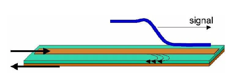
Signal integrity refers to the preservation of signal quality throughout its propagation across a PCB. In high-speed PCB design, signals operating at gigabit-per-second rates are particularly susceptible to degradation. Military communication PCBs handle protocols requiring low bit error rates, making signal integrity a cornerstone of system reliability. Factors like crosstalk, reflections, and attenuation can degrade signals, leading to timing errors or complete failures. Why does this matter? In battlefield scenarios, even brief communication lapses can have severe consequences, underscoring the need for robust design practices from the outset.
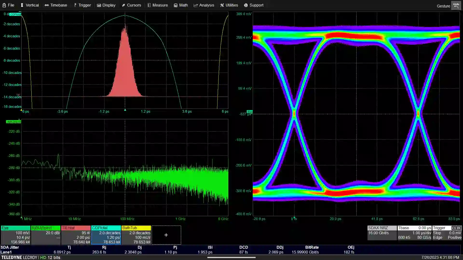
Transmission line effects emerge prominently when signal rise times approach or exceed the propagation delay of PCB traces. At high frequencies, traces behave as transmission lines rather than simple wires, introducing phenomena such as ringing and overshoot. Engineers must model these effects accurately to predict and mitigate issues. Poor management leads to eye diagram closure, where signal margins vanish. In military systems, where data throughput is paramount, ignoring transmission line effects risks operational failure.
Core Technical Principles in High-Speed PCB Design
High-speed PCB design hinges on understanding transmission line theory. Every PCB trace has a characteristic impedance determined by its width, thickness, height above reference planes, and dielectric properties. Mismatches in this impedance cause reflections, distorting the waveform. Impedance control involves precise stackup design and material selection to maintain consistent values, typically 50 ohms for single-ended or 100 ohms for differential pairs. As outlined in IPC-2221 guidelines, conductor spacing and routing rules help preserve impedance uniformity across the board. For defense applications, a symmetric multilayer configuration is essential—refer to our guide on Optimizing PCB Stack Up for High Speed Signals for detailed layer examples.
Transmission line effects intensify with frequency, where skin effect confines current to trace surfaces, increasing effective resistance. Dielectric losses from material dissipation further attenuate signals. Engineers analyze these using time-domain reflectometry (TDR) simulations to visualize impedance profiles. Controlling via stubs and bends minimizes discontinuities. In military communication PCBs, where trace lengths can span multiple inches, these principles prevent cumulative degradation over long paths.
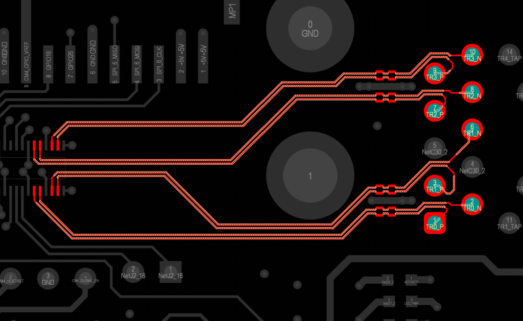
Differential signaling enhances signal integrity by transmitting data as complementary pairs. This technique rejects common-mode noise, crucial in noisy military environments. Pair skew, the timing difference between signals, must stay below a fraction of the bit period. SerDes (Serializer/Deserializer) interfaces, common in high-speed links, leverage differential pairs for rates exceeding 10 Gbps. Proper length matching and coupling maintain balance. These methods reduce electromagnetic emissions, aiding compliance with electromagnetic compatibility requirements.
Material Selection for Harsh Military Environments
Material choice is paramount in military high-speed PCB design because thermal cycling, vibration, and humidity directly impact dielectric constant (Dk) stability, loss tangent (Df), and mechanical integrity.
Material Comparison Table
| Material | Dk (10 GHz) | Df (10 GHz) | Tg (°C) | CTE (ppm/°C) | Vibration Resistance | Relative Cost | Best Military Applications |
|---|---|---|---|---|---|---|---|
| Standard FR-4 | 4.3–4.7 | 0.018–0.022 | 130–150 | 14–18 | Low | Low | Non-critical digital sections |
| Rogers RO4350B | 3.48 | 0.0037 | >280 | 10–14 | Medium-High | Medium | High-speed digital, radar interfaces |
| Megtron 6 (Panasonic) | 3.4–3.6 | 0.002 | 185–200 | 11–13 | High | Medium-High | Backplanes, secure comms modules |
| Rogers RT/duroid 5880 | 2.20 | 0.0009 | N/A (PTFE) | 10–20 (Z-axis critical) | Very High | High | RF/microwave links, antenna feeds |
| PTFE-based hybrids | 2.1–3.0 | <0.0015 | >200 | 12–25 | Excellent | Very High | Extreme environment MIL-STD-810 systems |
Hybrid constructions—pairing low-loss PTFE or Rogers cores for high-speed layers with standard materials in non-critical areas—optimize both electrical performance and cost. These materials maintain stable Dk under temperature swings from –55 °C to +125 °C and resist delamination during vibration testing.
Practical Solutions: Termination Techniques and Impedance Control
Termination techniques address reflections at line ends. Series termination places a resistor near the driver to match source impedance, damping overshoot without power penalties. Parallel termination at the receiver absorbs incoming waves but draws DC current. For military PCBs, AC termination using capacitors avoids steady-state power loss while providing high-frequency matching. Selection depends on topology: daisy-chain suits multi-drop buses, while point-to-point favors simpler stubs.
Impedance control starts with stackup optimization. Symmetric multilayer stacks with dedicated power and ground planes provide return paths, reducing inductance. Material choices influence dielectric constant and loss tangent, directly impacting signal propagation. Vias introduce discontinuities; blind or buried vias minimize stubs. Routing high-speed nets on inner layers shields them from external interference. Pre-layout simulations verify control before fabrication.
In high-speed PCB design, length matching for differential pairs prevents skew-induced errors. Meander structures equalize paths without excessive coupling. Ground clearance around traces avoids parasitic capacitance. For SerDes channels, equalization compensates losses, with pre-emphasis boosting high frequencies at the transmitter. These practices ensure open eye diagrams, quantifying signal integrity margins.
Advanced Best Practices for Military Communication PCBs
Military environments demand extras beyond standard high-speed PCB design. Thermal management prevents coefficient mismatches that warp boards, altering impedance. Vibration-resistant vias and anchors secure traces. IPC-A-610 Class 3 criteria ensure high-reliability assemblies, specifying tolerances for plating and solder joints. Conformal coatings protect against humidity, preserving dielectric integrity. Engineers should also review specialized material choices in our article on PTFE PCBs in Aerospace and Defense: Meeting the Demands of Extreme Environments.
Routing strategies prioritize critical nets first. Orthogonal routing between layers reduces crosstalk. Via fencing around high-speed areas contains fields. Power distribution networks with decoupling capacitors suppress simultaneous switching noise. Post-layout extraction models full-wave effects for final verification. These steps optimize signal integrity holistically.
SerDes implementation requires clock-data recovery circuits tolerant to jitter. Forward error correction adds redundancy for long-haul links. Testing involves bit error rate measurements under stress. In military PCBs, qualification per IPC-6012 verifies performance across lifecycle conditions. Integrating these ensures systems withstand deployment rigors.
Design Challenges and Troubleshooting Insights
Common pitfalls in high-speed PCB design include inadequate plane splits, causing return path detours and increased noise. Engineers troubleshoot with TDR to pinpoint mismatches. Excessive vias degrade SerDes performance; minimizing count or using back-drills resolves this. Crosstalk from adjacent aggressor lines mandates spacing rules. Simulations correlate with hardware measurements for iterative refinement.
In military applications, environmental stressors exacerbate issues. Temperature cycling alters dielectric constants, shifting impedance. Mechanical shock induces microcracks in traces. Proactive derating and margin analysis mitigate risks. Case in point: redesigning a communication module involved tightening impedance tolerances and adding shielding, restoring signal margins.
DFM, Manufacturability & SWaP Considerations for Defense
Defense projects impose strict SWaP constraints. Early fabricator engagement ensures design rules align with production capabilities—particularly for hybrid stacks, back-drilling, and tight registration. DFM reviews address etch uniformity (±0.5 mil), material handling for PTFE, and cost drivers such as sequential lamination cycles. Balancing performance with manufacturability reduces scrap rates and accelerates time-to-deployment for military programs.
Conclusion
High-speed PCB design for military communication PCBs centers on signal integrity to enable reliable data transmission. Mastering transmission line effects, impedance control, termination techniques, differential signaling, and SerDes ensures robust performance. Structured approaches, from stackup to verification, align with industry best practices. By prioritizing these elements, engineers deliver systems that perform under extreme conditions. Future advancements in materials will further enhance capabilities, but foundational principles remain timeless.
FAQs
Q1: What role do transmission line effects play in high-speed PCB design?
A1: Transmission line effects occur when signal wavelengths approach trace lengths, causing reflections and distortions. In military communication PCBs, they degrade signal integrity at gigabit speeds. Engineers model traces as controlled-impedance lines to predict behavior. Mitigation involves matching source, load, and line impedances. Proper analysis prevents bit errors in critical links.
Q2: How does impedance control improve signal integrity?
A2: Impedance control maintains consistent trace characteristics, minimizing reflections in high-speed PCB design. Stackups with precise layer thicknesses and dielectrics achieve target values like 100 ohms differential. Simulations guide routing to avoid discontinuities. In military applications, it ensures low jitter for SerDes channels. Verification via TDR confirms uniformity.
Q3: What are effective termination techniques for high-speed signals?
A3: Termination techniques match impedances to absorb reflections, preserving signal integrity. Series resistors damp overshoot near drivers, while parallel options suit receivers. AC termination balances power and performance. For differential signaling, Thevenin networks provide balanced matching. Selection aligns with topology and speed requirements in military PCBs.
Q4: Why is differential signaling preferred in military communication PCBs?
A4: Differential signaling uses paired traces to reject noise, vital for signal integrity in harsh environments. It supports high speeds in SerDes interfaces with low emissions. Length matching controls skew for timing accuracy. Common-mode rejection enhances reliability. This approach outperforms single-ended in electromagnetic interference-prone settings.
References
IPC-2221 — Generic Standard on Printed Board Design. IPC
IPC-A-610 — Acceptability of Electronic Assemblies. IPC
IPC-6012E — Qualification and Performance Specification for Rigid Printed Boards. IPC, 2015


