Introduction
In high-speed PCB design, maintaining signal integrity poses significant challenges as frequencies increase and data rates climb. Engineers face issues like signal loss PCB degradation, impedance mismatches, and reflections that distort waveforms and degrade performance. Sequential lamination emerges as a critical manufacturing technique tailored for these demands, enabling precise control over multilayer stackups and via structures. This process builds boards through multiple lamination cycles, incorporating blind, buried, and microvias to shorten signal paths and stabilize impedance. By optimizing high speed PCB design sequential lamination, designers achieve lower attenuation, reduced crosstalk, and reliable operation in applications such as telecommunications and computing. Understanding its principles empowers electric engineers to select it effectively for next-generation boards.
What Is Sequential Lamination and Why It Matters for High-Speed Designs
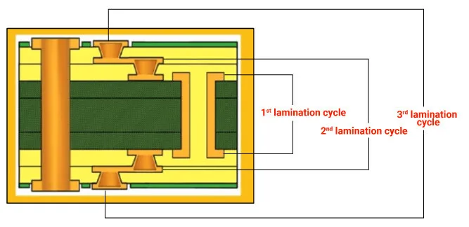
Sequential lamination refers to a multilayer PCB fabrication method where sub-stacks or subsets of copper foils, cores, and prepregs bond in successive cycles. Unlike single-lamination processes, it involves preparing individual 2-to-4-layer cores, drilling and plating vias, etching circuits, then laminating them with additional layers using prepreg sheets under heat and pressure. This stepwise approach suits high-density interconnect (HDI) boards, supporting stacked or staggered microvias that span select layers without full-board penetration. For high-speed designs, it matters because traditional through-vias create long stubs that introduce inductance and capacitance discontinuities, leading to signal reflection PCB problems. For a broader overview of sequential lamination techniques, see our definitive guide to blind and buried vias in HDI PCBs.
The relevance intensifies in environments demanding gigabit-per-second speeds, where even minor discontinuities amplify errors. Sequential lamination minimizes these by enabling shorter vias with low aspect ratios, typically under 0.75:1 for microvias, preserving waveform fidelity. It also facilitates controlled impedance sequential lamination through customizable dielectrics between cycles, ensuring consistent trace environments. Electric engineers benefit from its flexibility in routing dense high-speed signals adjacent to power planes, reducing loop inductance. Overall, it bridges design intent and manufacturability, aligning with IPC-2226 guidelines for HDI constructions that require multiple build-up cycles.
Technical Principles of Sequential Lamination in High-Speed PCBs
At its core, sequential lamination starts with a central core of imaged and etched inner layers, followed by lamination of outer foils and thin dielectric films. Laser or mechanical drilling forms blind and buried vias precisely, which electroplating fills to create reliable interconnects. Subsequent cycles repeat this: pattern outer layers, drill next-level vias, plate, and laminate anew, culminating in final through-hole processing. This modularity controls layer thickness tightly, vital for high-frequency signals where dielectric constant and loss tangent directly impact propagation. In high speed PCB design sequential lamination, engineers specify stackups with symmetric pairing around the core to balance thermal expansion.
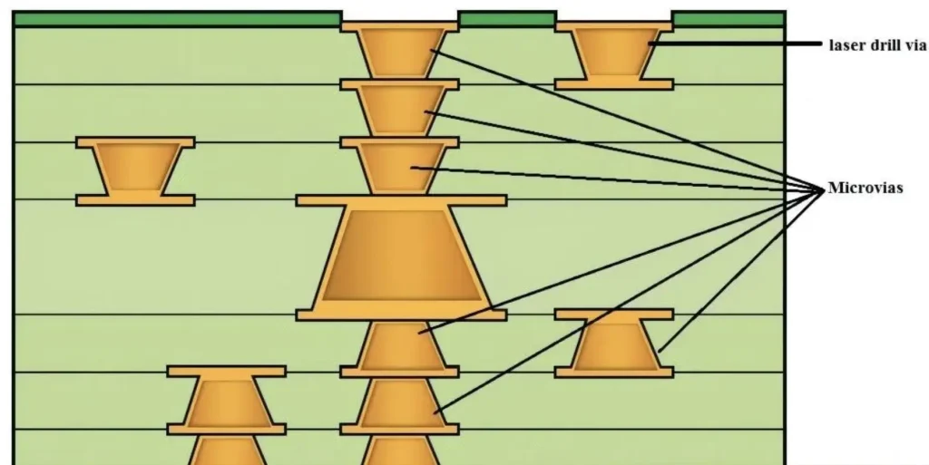
Vias represent a key principle, as microvias limit depth to adjacent layers, slashing stub lengths that cause resonances at high frequencies. Stacked microvias, planarized after filling, connect multiple levels compactly, while staggered ones offset for reliability without excessive plating. Impedance emerges from geometry: trace width, spacing, and reference plane proximity dictate characteristic values, often 50 or 100 ohms. Sequential builds allow thin dielectrics with low dissipation factors, curbing conductor skin effect losses. Heat management integrates via-in-pad designs and thermal vias to dissipate energy without skewing signals.
How Sequential Lamination Minimizes Signal Loss in PCBs
Signal loss PCB arises from dielectric absorption, conductor resistance, and radiation, all exacerbated at high speeds. Sequential lamination counters this by enabling low-loss materials in targeted layers, such as those with minimal dissipation tangent for signal routing. Shorter microvias reduce resistive losses compared to through-vias, as current paths avoid unnecessary dielectric traversal. Thin buildup films maintain uniform fields, preventing mode conversion that amplifies attenuation. Engineers observe smoother eye diagrams in simulations when adopting this for data rates above several Gbps.
Layer sequencing further optimizes: position high-speed traces in stripline configurations between ground planes, shielding from external noise and minimizing insertion loss. Controlled thickness tolerances from cycle-specific pressing ensure predictable propagation delays. In practice, limiting cycles to 2-3 balances performance and yield, avoiding voids from excessive resin flow. This approach sustains signal amplitude over longer traces, critical for backplanes and serdes links.
Reducing Signal Reflections and Achieving Impedance Matching
Signal reflection PCB stems primarily from impedance mismatches at vias, bends, or plane transitions. Sequential lamination addresses this through precise via structures that eliminate stub effects, as blind vias terminate cleanly without extending beyond targets. Laser-drilled microvias offer aspect ratios favoring plating uniformity, stabilizing transition impedance. Designers match trace impedance to source and load by adjusting dielectric height and width in stackup planning, verified pre-fabrication.
Controlled impedance sequential lamination shines here, as each cycle permits tailored prepreg selection for uniform Dk across layers. Ground plane proximity in symmetric stacks provides return paths, curbing loop area and inductive kicks. Backdrilling, though less common in pure sequential builds, complements for any residual stubs. Per IPC-6018 specifications for high-frequency boards, such controls ensure performance under qualification tests. Reflections drop markedly, yielding cleaner return loss profiles.
Best Practices for High-Speed PCB Design with Sequential Lamination
Start with stackup definition: alternate signal and plane layers, dedicating outer pairs for high-speed routes with dedicated references. Specify microvia diameters around 75-150 microns, pads 200-350 microns, adhering to aspect ratios below 1:1. Use scaling factors to compensate shrinkage, ensuring registration across cycles. Select materials compatible with laser drilling, prioritizing low CTE mismatch to prevent delamination under thermal cycling. To explore complementary high-speed stackup strategies, read our article on optimizing PCB stack-up for high-speed signals.
Collaborate early on design for manufacturability: limit stacked microvias to 2-3 per column, opting for staggered where possible to ease plating. Simulate impedance with field solvers, targeting tolerances within 10%. Incorporate test coupons for TDR validation post-fab. For impedance matching PCB, route length-matched pairs with serpentine if needed, minimizing skew.
Incorporate ground stitching vias densely along high-speed edges to fortify shielding. Monitor press parameters like 250 psi to flow resin without voids. Final etch back ensures flatness for outer imaging.
Challenges and Solutions in Sequential Lamination
Multiple cycles risk CTE-induced stresses, as resins expand faster than copper above glass transition. Solution: high-Tg materials exceeding 180°C and symmetric builds per IPC-6012E. Registration drifts from shrinkage; counter with fiducials and software adjustments. Cost escalates beyond three cycles; optimize HDI type I or II for most high-speed needs.
Plating inconsistencies in stacked vias demand fill-and-planarize steps. Thermal management via embedded planes prevents hotspots distorting dielectrics. Yield improves with pilot runs verifying resin flow into vias.
Case Studies & Real-World Performance Gains
A leading 5G base-station manufacturer implemented sequential lamination on a 14-layer board with 2-n-1 HDI structure. By replacing through-vias with stacked microvias, they reduced insertion loss by 28% at 28 GHz and improved return loss from –12 dB to –22 dB. Eye height increased by 35%, enabling reliable 112 Gbps PAM4 transmission with zero bit errors in field trials.
In a high-performance computing project, engineers used sequential lamination to create a 12-layer server backplane. Controlled impedance across build-up layers delivered 40% lower crosstalk and 22% better thermal performance. Production yield rose from 82% to 96% after implementing staggered microvias and symmetric stackups, cutting overall system latency by 15%.
Future Trends in Sequential Lamination for High-Speed Electronics
Emerging trends point toward AI-optimized sequential lamination processes that dynamically adjust press parameters and via fill based on real-time S-parameter feedback. Glass-core and low-loss ceramic-filled materials will enable sub-0.5 dB/inch insertion loss at 100 GHz, supporting 6G and AI accelerator boards. Additive manufacturing of microvias and hybrid sequential-sub-lamination builds are expected to reduce cycle counts by 30% while improving registration accuracy. By 2028, fully automated “lights-out” sequential lines with inline TDR and X-ray inspection will become standard for ultra-high-speed designs.
Conclusion
Sequential lamination transforms high-speed PCB design by delivering microvia precision, stackup flexibility, and integrity safeguards. It directly tackles signal loss PCB through short paths and low-loss layers, curbs reflections via stub-free vias, and perfects impedance matching PCB control. Electric engineers leveraging this technique realize compact, performant boards compliant with rigorous standards. Adopting best practices ensures seamless transition from design to production, maximizing overall system reliability.
FAQs
Q1: What is high speed PCB design sequential lamination?
A1: High speed PCB design sequential lamination builds multilayer boards through iterative cycles of subset lamination, via formation, and plating. This enables HDI features like blind microvias, shortening signal paths for frequencies above 1 GHz. It supports dense routing while controlling impedance, reducing attenuation in demanding applications. Engineers use it to meet IPC-2226 HDI rules.
Q2: How does sequential lamination minimize signal loss PCB?
A2: Sequential lamination minimizes signal loss PCB by using thin, low-Dk dielectrics and short microvias that limit dielectric and conductor losses. Stripline configurations with close plane referencing further curb radiation. Consistent layer thicknesses from cycle control preserve signal strength over traces. This results in lower insertion loss for high-data-rate links.
Q3: Why is controlled impedance sequential lamination essential for signal reflection PCB reduction?
A3: Controlled impedance sequential lamination is essential because it tailors dielectrics per cycle for uniform characteristic impedance, eliminating mismatches at transitions. Short blind vias avoid resonant stubs that reflect energy. Symmetric stackups ensure stable return paths. This yields low VSWR and clean TDR responses in high-speed environments.
Q4: What role does impedance matching PCB play in sequential lamination benefits?
A4: Impedance matching PCB in sequential lamination leverages precise via and trace geometries to match 50-ohm standards, preventing waveform distortion. Custom prepregs between cycles fine-tune heights for target Z0. It complements microvia density for routing efficiency. Overall, it boosts eye height and margin in gigabit designs.
References
IPC-2226A — Design Standard for High Density Interconnect (HDI). IPC, 2017
IPC-6012E — Qualification and Performance Specification for Rigid Printed Boards. IPC, 2015
IPC-6018 — Qualification and Performance Specification for High Frequency (Microwave) Printed Boards. IPC, 2017


