Introduction
Printed circuit boards (PCBs) form the backbone of modern electronics, where size selection directly impacts device performance, reliability, and market viability. Engineers face the challenge of PCB size considerations that must accommodate dense component placement while ensuring signal integrity and thermal stability. As consumer demand drives smaller form factors, PCB miniaturization techniques become essential, yet they introduce PCB design constraints like routing density and material limitations. This guide examines PCB size and functionality trade-offs, offering structured insights into PCB size optimization for electric engineers. By understanding these elements, designers can create boards that meet functional requirements without compromising manufacturability. Key factors include electrical pathways, heat management, and mechanical robustness, all intertwined with size decisions.
Why PCB Size Selection Matters in Modern Electronics
PCB size selection influences every stage from design to deployment, determining how well a board supports its intended application. Smaller sizes enable compact devices like wearables and IoT sensors, but they demand precise PCB miniaturization techniques to maintain functionality. Larger boards provide ample space for routing and components, reducing risks of crosstalk and overheating, yet they increase material costs and assembly complexity. PCB size considerations extend to regulatory compliance and end-user ergonomics, where oversized boards may hinder portability. In high-volume production, optimal sizing improves yield rates and minimizes defects like warpage. Ultimately, balancing PCB size and functionality ensures the board delivers reliable performance across diverse environments.
Electric engineers prioritize size for its role in system integration, where mismatched dimensions lead to enclosure fit issues or inefficient power distribution. Industry trends toward higher integration densities amplify these challenges, making PCB size optimization a core competency. Poor choices result in redesign iterations, escalating development timelines and expenses. Conversely, well-optimized sizes enhance scalability for future upgrades. This relevance underscores the need for systematic evaluation during initial concept phases.
Key Technical Principles Governing PCB Size
Electrical performance forms a foundational PCB size consideration, as trace lengths and layer counts directly affect signal propagation and impedance. Shorter traces in miniaturized designs reduce attenuation and electromagnetic interference, but they necessitate finer linewidths, pushing PCB design constraints on resolution limits. Vias and pads consume valuable real estate, so size must accommodate sufficient spacing per high-speed signal requirements. Engineers model these using transmission line theory to predict behavior across frequencies. Larger boards allow wider traces for current handling, mitigating voltage drops in power sections.
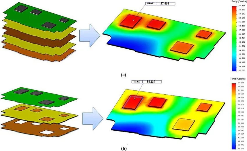
Thermal management represents another critical mechanism, where PCB size dictates heat spreading efficiency through copper planes and vias. Compact designs concentrate heat from dense ICs, risking junction temperatures that exceed component ratings. Extended sizes facilitate larger heatsinks or airflow paths, improving dissipation via convection and radiation. Material thermal conductivity and thickness interplay with area to define overall capacity. Simulations reveal hotspots, guiding size adjustments to prevent thermal runaway.
Mechanical stability arises from size-related stresses during fabrication and operation. Larger panels experience greater warpage due to coefficient of thermal expansion mismatches between copper and substrate, as governed by IPC-6012E specifications for rigid boards. Thinner, smaller boards offer flexibility but vulnerability to flexure-induced cracks. Aspect ratios, defined as board length to thickness, influence rigidity; excessive ratios amplify handling risks. Finite element analysis helps quantify these effects early.
PCB Design Constraints and Their Impact on Size
Fabrication constraints impose hard limits on achievable PCB sizes, starting with panel utilization and yield optimization. Standard panel sizes dictate how multiple boards fit, influencing per-unit costs; oversized designs waste edge material. Minimum feature sizes, such as drill diameters and annular rings, scale with complexity, compressing usable area in small boards. Aspect ratios for plating processes cap hole depths relative to diameters, constraining multilayer stackups in compact forms.
Material selection adds layers to PCB design constraints, as substrates vary in dimensional stability under humidity and temperature cycles. High-frequency laminates enable miniaturization but introduce higher costs and handling sensitivities. Copper weight balances current capacity against etch precision; heavier foils suit larger boards with high-power traces. Compliance with IPC-A-600K acceptability criteria ensures surfaces remain flat post-processing.
Assembly processes further shape size decisions, with pick-and-place machines favoring rectangular footprints under certain dimensions. Solder paste application via stencils demands flatness across the board area, where warpage from size exceeds PCB size tolerances. Reflow ovens impose zone lengths that align with conveyor speeds, indirectly limiting elongated designs. These constraints collectively drive PCB size optimization toward practical geometries.
PCB Miniaturization Techniques for Enhanced Functionality
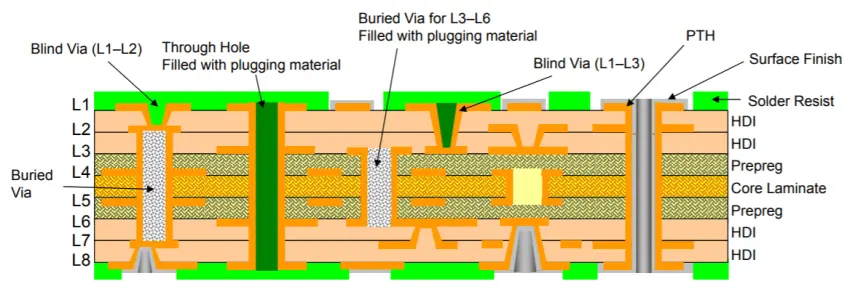
High-density interconnect (HDI) technology stands as a premier PCB miniaturization technique, employing microvias and blind vias to stack layers densely. This reduces overall footprint by routing signals vertically, freeing surface space for components. Laser-drilled vias enable finer pitches, supporting ball grid arrays with thousands of I/Os. Sequential build-up processes layer dielectrics progressively, achieving sub-100-micron features.
Embedded components integrate passives directly into substrates, slashing board area by eliminating surface mounts. Cavities or build-up films house capacitors and resistors, preserving signal paths. This technique demands precise control of tolerances to avoid parasitics. Fine-line imaging with laser direct imaging resolves traces below 50 microns, critical for high-speed interfaces.
Substrate-like PCB (SLP) approaches mimic IC packaging, using ultra-thin cores for near-chip-scale boards. Any-layer vias interconnect every layer without skips, maximizing density. These methods navigate PCB design constraints through advanced materials like low-loss dielectrics.
Panelization strategies multiply small boards on carriers, optimizing production despite tiny individual sizes. Fiducials and breakaway tabs ensure alignment during depaneling.
Best Practices for PCB Size Optimization
Begin PCB size optimization with requirements capture, mapping functional blocks to spatial allocations via block diagrams. Allocate margins for routing channels, typically 10-20% of component outlines, adjusting iteratively. Parametric studies in design software explore trade-offs between size and layer count.
Incorporate design for manufacturability (DFM) by adhering to fabricator guidelines on outline shapes and tab placements. Rectangular or near-rectangular forms maximize panel efficiency. Simulate warpage using J-STD-020E reflow profiles to predict size-induced distortions.
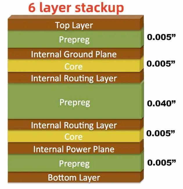
Layer stackup planning balances size with impedance control; symmetric builds minimize bow and twist. Thermal vias under hot components distribute heat without expanding footprint. Prototype iterations validate assumptions, refining PCB size considerations.
Collaborate across disciplines: electrical for signals, thermal for dissipation, mechanical for enclosures. Document rationale in design reviews to institutionalize best practices.
Case Studies in Balancing Size and Functionality
Consider a handheld medical device requiring dense analog front-ends; initial 100x80 mm design suffered signal noise from long traces. Miniaturization to 60x50 mm via HDI cut noise by 30%, fitting tighter enclosures while upholding functionality. Warpage stayed below 0.75% per IPC specs through balanced copper distribution.
In automotive ECUs, size grew to 150x100 mm for power modules, enhancing thermal margins without vias overload. Optimization partitioned high-current sections, preserving signal isolation. These examples highlight PCB size and functionality harmony through targeted techniques.
A server backplane case scaled to 300x200 mm for connector density, using rigid-flex hybrids to fold efficiently. This navigated constraints, boosting port count 50%.
Conclusion
PCB size selection demands a holistic approach, weighing electrical, thermal, and mechanical PCB size considerations against miniaturization goals. Techniques like HDI and embedding enable compact designs without sacrificing functionality, while optimization practices ensure manufacturability. Engineers mastering these elements achieve robust, efficient boards tailored to applications. Prioritize simulations and standards compliance for repeatable success. As electronics evolve, adept PCB size optimization remains pivotal for innovation.
FAQs
Q1: What are the primary PCB size considerations for electric engineers?
A1: Key PCB size considerations include electrical signal integrity, thermal dissipation capacity, and mechanical stability against warpage. Trace lengths affect impedance, while area influences heat spreading via copper planes. Fabrication limits on features and panelization impact feasibility. Balancing these ensures functionality in constrained spaces, guided by standards like IPC-6012E.
Q2: How does PCB size influence functionality in high-density designs?
A2: PCB size and functionality link through routing density and component spacing; smaller sizes demand finer features to avoid crosstalk. Heat concentration rises, potentially degrading performance unless mitigated by vias. Larger sizes support robust power delivery but challenge portability. Optimization via stackups maintains integrity across scales.
Q3: What PCB miniaturization techniques best address design constraints?
A3: Effective PCB miniaturization techniques encompass HDI with microvias, embedded passives, and SLP structures. These reduce footprint by vertical integration and substrate embedding, easing PCB design constraints on surface area. Laser drilling and fine-line etching enable high densities. Validation through prototypes confirms reliability.
Q4: How can engineers achieve PCB size optimization without compromising quality?
A4: PCB size optimization starts with block diagramming and DFM checks, simulating thermal and warpage effects. Symmetric stackups and panelization maximize yield. Iterative prototyping refines dimensions per IPC-A-600K criteria. Cross-disciplinary reviews align size with functionality goals.
References
IPC-6012E — Qualification and Performance Specification for Rigid Printed Boards. IPC, 2018
IPC-A-600K — Acceptability of Printed Boards. IPC, 2020
J-STD-020E — Moisture/Reflow Sensitivity Classification of Nonhermetic Surface Mount Devices. JEDEC/IPC, 2014


